
Catalog excerpts

■ Period Range: 1ms to 9.5 Hours ■ Timing Reset by Power-On or Reset Input ■ Configured with 1 to 3 Resistors ■ <1.5% Maximum Frequency Error ■ Programmable Output Polarity ■ 2.25V to 5.5V Single Supply Operation ■ CMOS Output Driver Sources/Sinks 20mA ■ -55°C to 125°C Operating Temperature Range ■ Available in Low Profile (1mm) SOT-23 (ThinSOT™) ■ Power-On Reset Timer ■ Long Time One Shot ■ Periodic "Wake-Up" Call ■ High Vibration, High Acceleration Environments XT, LT, LTC, LTM, Linear Technology, TimerBlox and the Linear logo are registered trademarks and ThinSOT is a trademark of Linear Technology Corporation. All other trademarks are the property of their respective owners. TimerBlox: Long Timer, Low Frequency Oscillator The LTC®6995 is a silicon oscillator with a programmable period range of 1.024msto 9.54 hours (29.1 uHzto977Hz), specifically intended for long duration timing events. The LTC6995 is part of the TimerBlox® family of versatile silicon timing devices. A single resistor, RSEL programs the LTC6995's internal master oscillator frequency. The output clock period is determined by this master oscillator and an internal frequency divider, NQIV. programmable to eight settings NpiV *RsET When oscillating, the LTC6995 generates a 50% duty cycle square wave output. A reset function is provided to stop the master oscillator and clear internal dividers. Removing reset initiates a full output clock cycle which is useful for programmable power on reset and watchdog timer applications. The LTC6995 has two versions of reset functionality. The reset input is active high forthe LTC6995-1 and active low for the LTC6995-2. The polarity of the output when reset is selectable for both versions. TVPicni nppucnTion Active Low Power-On Reset Timer POWER-ON RESET TIMER STOPPED ^^^J TECHNOLOGY
Open the catalog to page 1
ABSOLUTE mnximum Rnnnos Maximum Voltage Operating Temperature Range (Note 2) Specified Temperature Range (Note 3) Lead Temperature (Soldering, 10 sec) ORD€R inFORmnnon Lead Free Finish TRM = 500 pieces. "Temperature grades are identified by a label on the shipping container. Consult LTC Marketing for parts specified with wider operating temperature ranges. Consult LTC Marketing for information on lead based finish parts. For more information on lead free part marking, go to: http://www.linear.com/leadfree/ For more information on tape and reel specifications, go to:...
Open the catalog to page 2
The • denotes the specifications which apply over the full operating temperature range, otherwise specifications are at TA = 25°C. Test conditions are V+ = 2.25V to 5.5V, RST = 0V for LTC6995-1, RST = V+ for LTC6995-2, DIVCODE = 0 to 15 (Nmv = 1 to 221), RSET = 50k to 800k, RLOAD = 5k, CLQAD = 5pF unless otherwise noted. Analog Inputs ^^^J TECHNOLOGY
Open the catalog to page 3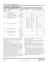
The • denotes the specifications which apply over the full operating temperature range, otherwise specifications are at TA = 25°C. Test conditions are V+ = 2.25V to 5.5V, RST = OV for LTC6995-1, RST = V+ for LTC6995-2, DIVCODE = 0 to 15 (Nmv = 1 to 221), RSET = 50k to 800k, RLOAD =00. CLOAD = 5pF unless otherwise noted. Note 1: Stresses beyond those listed under Absolute Maximum Ratings may cause permanent damage to the device. Exposure to any Absolute Maximum Rating condition for extended periods may affect device Note 2: The LTC6995C is guaranteed functional over the operating Note 3: The...
Open the catalog to page 4
TVPicni p€RFonmnnc€ CHnnnacRisTics V+ = 3.3V, RSET = 200k, TA = 25°C unless otherwise noted. Frequency Error vs Temperature Frequency Error vs Temperature Frequency Error vs Temperature Frequency Error vs RSET VSET Drift VS ISET Frequency Drift vs Supply Voltage VSET Drift vs Supply Typical VSET Distribution VSETVS Temperature ^^^J TECHNOLOGY
Open the catalog to page 5
LTC6995-1/LTC6995-2 Typical Performance Characteristics + V = 3.3V, RSET = 200k, TA = 25°C unless otherwise noted. Supply Current vs Supply Voltage 150 125 100 RSET = 100k RSET = 200k 75 RSET = 800k 50 25 2 3 4 5 SUPPLY VOLTAGE (V) 250 125 5V, RSET = 100k 100 2.5V, RSET = 100k 75 5V, RSET = 800k 50 2.5V, RSET = 800k 25 0 –50 –25 6 50 25 75 0 TEMPERATURE (°C) 150 1000 V+ = 2.5V 0 200 400 RSET (kΩ) 600 600 400 0 800 2 3 4 5 SUPPLY VOLTAGE (V) 20 15 10 2 4 3 5 SUPPLY VOLTAGE (V) 6 NEGATIVE-GOING 1.5 1.0 2 3 4 5 SUPPLY VOLTAGE (V) 200 CLOAD = 5pF 65 UNITS SOT-23 AND DFN PARTS TA = 30°C 150 2.0...
Open the catalog to page 6
TVPicni P€RFORmnnc€ cHiMnacRisTics V+ = 3.3V, RSET = 200k, TA = 25°C unless otherwise noted. Output Resistance Typical LTC6995-1 Start-Up with RESET RELEASED, V+(Pin1/Pin5): Supply Voltage (2.25V to 5.5V). This sup- ply should be kept free from noise and ripple. It should be bypassed directly to the GND pin with a 0.1 uF capacitor. DIV (Pin 2/Pin 4): Programmable Divider and Polarity Input. An internal A/D converter (referenced to V+) moni- tors the DIV pin voltage (VQIV) to determine a 4-bit result (DIVCODE). VQIV may be generated by a resistor divider between V+ and GND. Use 1 % resistors...
Open the catalog to page 7
LTC6995-1/LTC6995-2 Pin Functions (DCB/S6) GND (Pin 5/Pin 2): Ground. Tie to a low inductance ground plane for best performance. 30Ω. When driving an LED or other low impedance load a series output resistor should be used to limit source/ sink current to 20mA. OUT (Pin 6/Pin 6): Oscillator Output. The OUT pin swings from GND to V+ with an output resistance of approximately Block Diagram (S6 package pin numbers shown) 5 V+ R1 4 DIV 4-BIT A/D CONVERTER POL BIT DIGITAL FILTER R2 MASTER OSCILLATOR 1µs V = SET 50kΩ ISET tMASTER = HALT OSCILLATOR OUTPUT IF ISET < 500nA MCLK FIXED DIVIDER ÷ 1024...
Open the catalog to page 8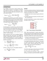
LTC6995-1/LTC6995-2 Operation The LTC6995 is built around a master oscillator with a 1MHz maximum frequency. The oscillator is controlled by the SET pin current (ISET) and voltage (VSET), with a 1MHz • 50k conversion factor that is accurate to ±0.8% under typical conditions. fMASTER = 1 tMASTER I = 1MHz • 50kΩ • SET VSET A feedback loop maintains VSET at 1V ±30mV, leaving ISET as the primary means of controlling the output frequency. The simplest way to generate ISET is to connect a resistor (RSET) between SET and GND, such that ISET = VSET/RSET . The master oscillator equation reduces to:...
Open the catalog to page 9All ADI catalogs and technical brochures
-
 LTC2068
30 Pages
-
 LTC6373
34 Pages
-
 ADL9006
16 Pages
-
 ADL8104
23 Pages
-
 AD4115
52 Pages
-
 ADUM7702
22 Pages
-
 AD7383
33 Pages
-
 AD7384
33 Pages
-
 AD4114
49 Pages
-
 ADUM7704
22 Pages
-
 AD7134
86 Pages
-
 LTspice IV
53 Pages
-
 New Products Catalog
43 Pages
-
 RF/IF Amplifiers
9 Pages
-
 SAR ADC Drivers
2 Pages
-
 SmartMesh Brochure
8 Pages
-
 INDUSTRIAL SIGNAL CHAIN
24 Pages
-
 AUTOMOTIVE ELECTRONIC SOLUTIONS
48 Pages
-
 Battery Management Solutions
32 Pages
-
 DC/DC uModule Power Products
32 Pages
-
 Wireless & RF Solution
36 Pages
-
 LT6656 - 1
18 Pages


Archived catalogs
-
 New Products Catalog
39 Pages
-
 Power Management for LEDs
24 Pages
-
 High Speed ADC Products Brochure
14 Pages


