
Catalog excerpts
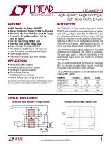
LTC4440A-5 High Speed, High Voltage, High Side Gate Driver Features The LTC®4440A-5 is a high frequency high side N-channel MOSFET gate driver that is designed to operate in applications with VIN voltages up to 80V. The LTC4440A-5 can also withstand and continue to function during 100V VIN transients. The powerful driver capability reduces switching losses in MOSFETs with high gate capacitances. The LTC4440A-5’s pull-up has a peak output current of 1.1A and its pull-down has an output impedance of 1.85Ω. Wide Operating VIN Range: Up to 80V Rugged Architecture Tolerant of 100V VIN Transients Powerful 1.85Ω Driver Pull-Down (with 6V Supply) Powerful 1.1A Peak Current Driver Pull-Up (with 6V Supply) 7ns Fall Time Driving 1000pF Load 10ns Rise Time Driving 1000pF Load Drives Standard Threshold MOSFETs TTL/CMOS Compatible Inputs with Hysteresis Input Thresholds are Independent of Supply Undervoltage Lockout Thermally Enhanced 8-Lead MSOP Package The LTC4440A-5 features supply independent TTL/CMOS compatible input thresholds with 350mV of hysteresis. The input logic signal is internally level-shifted to the bootstrapped supply, which may function at up to 95V above ground. The LTC4440A-5 is optimized for driving (5V) logic level FETs and contains an undervoltage lockout circuit that disables the external MOSFET when activated. Automotive Power Systems Telecommunications Power Systems Distributed Power Architectures Server Power Supplies High Density Power Modules General Purpose Low or High Side Driver The LTC4440A-5 is available in the thermally enhanced 8-lead MSOP package. L, LT, LTC, LTM, Linear Technology and the Linear logo are registered trademarks and Direct Flux Limit is a trademark of Linear Technology Corporation. All other trademarks are the property of their respective owners. Protected by U.S. Patents, including 6677210. PARAMETER Max Operating TS Absolute Max TS MOSFET Gate Drive VCC UV+ VCC UV– Typical Application Synchronous Phase-Modulated Full-Bridge Converter LTC4440A-5 Driving a 1000pF Capacitive Load
Open the catalog to page 1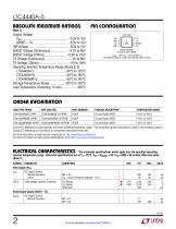
LTC4440A-5 Absolute Maximum Ratings (Note 1) MS8E PACKAGE 8-LEAD PLASTIC MSOP TJMAX = 150°C, θJA = 40°C/W (NOTE 4) EXPOSED PAD (PIN 9) IS GND, MUST BE SOLDERED TO PCB Order Information LEAD FREE FINISH PART MARKING* PACKAGE DESCRIPTION TEMPERATURE RANGE Consult LTC Marketing for parts specified with wider operating temperature ranges. *The temperature grade is identified by a label on the shipping container. Consult LTC Marketing for information on nonstandard lead based finish parts. For more information on lead free part marking, go to: http://www.linear.com/leadfree/ For more information...
Open the catalog to page 2
LTC4440A-5 Electrical Characteristics The ● denotes specifications which apply over the specified operating junction temperature range, otherwise specifications are at TA = 25°C. VCC = VBOOST = 6V, VTS = GND = 0V, unless otherwise noted. (Note 2) SYMBOL PARAMETER High Input Threshold Input Voltage Hysteresis Input Pin Bias Current Output Gate Driver (TG) VOH High Output Voltage Peak Pull-Up Current Output Pull-Down Resistance Output Rise Time Output Fall Time Output Low-High Propagation Delay Output High-Low Propagation Delay Note 1: Stresses beyond those listed under Absolute Maximum...
Open the catalog to page 3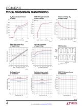
LTC4440A-5 Typical Performance Characteristics VCC Supply Quiescent Current vs Voltage BOOST-TS Supply Quiescent Current vs Voltage 300 HIGH OUTPUT VOLTAGE (V) VCC Supply Current vs Temperature VCC Undervoltage Lockout Thresholds vs Temperature BOOST-TS Quiescent Current vs Temperature 3.4 UVLO THRESHOLD VOLTAGE (V) Input (INP) Thresholds vs Supply Voltage Output High Voltage (VOH) vs Supply Voltage BOOST-TS SUPPLY VOLTAGE (V) 4440A5 G01 INP = VCC OUTPUT (TG-TS) VOLTAGE (mV) Output Low Voltage (VOL) vs Supply Voltage
Open the catalog to page 4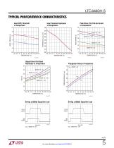
LTC4440A-5 Typical Performance Characteristics Input (INP) Threshold vs Temperature 380 Output Driver Pull-Down Resistance vs Temperature Propagation Delay vs Temperature Peak Driver (TG) Pull-Up Current vs Temperature Input Threshold Hysteresis vs Temperature Driving a 3300pF Capacitive Load Driving a 3300pF Capacitive Load
Open the catalog to page 5
LTC4440A-5 Pin Functions INP (Pin 1): Input Signal. TTL/CMOS compatible input referenced to GND (Pin 2). GND (Pins 2, 4, Exposed Pad Pin 9): Ground. The exposed pad must be electrically connected to Pins 2 and 4 and soldered to PCB ground for rated thermal performance. VCC (Pin 3): Chip Supply. This pin powers the internal low side circuitry. A low ESR ceramic bypass capacitor should be tied between this pin and the GND pin (Pin 2). NC (Pin 5): No Connect. No connection required. For convenience, this pin may be tied to Pin 6 (BOOST) on the application board. BOOST (Pin 6): High Side...
Open the catalog to page 6
LTC4440A-5 Applications Information Overview The LTC4440A-5 receives a ground-referenced, low voltage digital input signal to drive a high side N-channel power MOSFET whose drain can float up to 80V above ground, eliminating the need for a transformer between the low voltage control signal and the high side gate driver. The LTC4440A-5 normally operates in applications with input supply voltages (VIN) up to 80V, but is able to withstand and continue to function during 100V, 100ms transients on the input supply. The powerful output driver of the LTC4440A-5 reduces the switching losses of the...
Open the catalog to page 7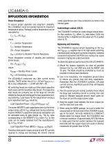
LTC4440A-5 Applications Information Power Dissipation To ensure proper operation and long-term reliability, the LTC4440A-5 must not operate beyond its maximum temperature rating. Package junction temperature can be calculated by: nodal capacitances and cross-conduction currents in the internal gates. Undervoltage Lockout (UVLO) The LTC4440A-5 contains an undervoltage lockout detector that monitors VCC. When VCC falls below 3.04V, the internal buffer is disabled and the output pin TG is pulled down to TS. TA = Ambient Temperature PD = Power Dissipation θJA = Junction-to-Ambient Thermal...
Open the catalog to page 8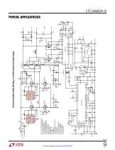
UVLO VREF ADLY PDLY CT SPRG RLEB FB GND PGND 24 GND-F GND-S OUTA OUTB OUTC OUTD OUTF OUTE LTC3722/LTC4440A-5 420W 36V-60VIN to 12V/35A Isolated Full-Bridge Supply Typical Applications
Open the catalog to page 9All ADI catalogs and technical brochures
-
 LTC2068
30 Pages
-
 LTC6373
34 Pages
-
 ADL9006
16 Pages
-
 ADL8104
23 Pages
-
 AD4115
52 Pages
-
 ADUM7702
22 Pages
-
 AD7383
33 Pages
-
 AD7384
33 Pages
-
 AD4114
49 Pages
-
 ADUM7704
22 Pages
-
 AD7134
86 Pages
-
 LTspice IV
53 Pages
-
 New Products Catalog
43 Pages
-
 RF/IF Amplifiers
9 Pages
-
 SAR ADC Drivers
2 Pages
-
 SmartMesh Brochure
8 Pages
-
 INDUSTRIAL SIGNAL CHAIN
24 Pages
-
 AUTOMOTIVE ELECTRONIC SOLUTIONS
48 Pages
-
 Battery Management Solutions
32 Pages
-
 DC/DC uModule Power Products
32 Pages
-
 Wireless & RF Solution
36 Pages
-
 LT6656 - 1
18 Pages


Archived catalogs
-
 New Products Catalog
39 Pages
-
 Power Management for LEDs
24 Pages
-
 High Speed ADC Products Brochure
14 Pages


