
Catalog excerpts

LTC4227-1/LTC4227-2 1 422712f Typical Application Features Description Dual Ideal Diode and Single Hot Swap Controller The LTC®4227 offers ideal diode and Hot Swap™ functions for two power rails by controlling external N-channel MOSFETs. MOSFETs acting as ideal diodes replace two high power Schottky diodes and the associated heat sinks, saving power and board area. A Hot Swap control MOSFET allows a board to be safely inserted and removed from a live backplane by limiting inrush current. The supply output is also protected against short-circuit faults with a fast acting current limit and internal timed circuit breaker. The LTC4227 regulates the forward voltage drop across the MOSFETs to ensure smooth current transfer from one supply to the other without oscillation. The ideal diodes turn on quickly to reduce the load voltage droop during supply switchover. If the input supply fails or is shorted, a fast turn-off minimizes reverse-current transients. The LTC4227 allows turn-on/off control, and reports fault and power good status for the supply. The LTC4227-1 features a latch-off circuit breaker, while the LTC4227-2 provides automatic retry after a fault. Diode-OR with Hot Swap Application Applications n Power Path and Inrush Current Control for Redundant Supplies n Low Loss Replacement for Power Schottky Diodes n Allows Safe Hot Swapping from a Live Backplane n 2.9V to 18V Operating Range n Controls N-Channel MOSFETs n Limits Peak Fault Current in 1ìs n 0.5ìs Turn-On and Reverse Turn-Off Time n Adjustable Current Limit with Circuit Breaker n Smooth Switchover without Oscillation n Adjustable Current Limit Fault Delay n Fault and Power Status Output n LTC4227-1: Latch Off After Fault n LTC4227-2: Automatic Retry After Fault n 20-Lead 4mm × 5mm QFN and 16-Lead SSOP Packages n Redundant Power Supplies n Supply Holdup n Computer Systems and Servers n Telecom Networks L, LT, LTC, LTM, Linear Technology and the Linear logo are registered trademarks of Linear Technology Corporation. Hot Swap is a trademark of Linear Technology Corporation. All other trademarks are the property of their respective owners. BACKPLANE CONNECTOR 12V 12V CARD CONNECTOR CPO1 D2ON ON FAULT PWRGD 137k 100ìF 12V 7.6A 20k INTVCC GND IN1 DGATE1 DGATE2 LTC4227 422712 TA01a SiR462DP 0.006 Si7336ADP CPO2 SENSE+ SENSE– HGATE OUT 0.1ìF IN2 + 0.1ìF SiR462DP EN 0.1ìF 0.1ìF TMR Power Dissipation vs Load Current LOAD CURRENT (A) 0 0 POWER DISSIPATION (W) 0.5 1.0 1.5 2.0 2.5 3.0 2 4 6 8 4227 TA01 DIODE (SBG1025L) MOSFET (SiR462DP) POWER SAVED
Open the catalog to page 1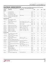
LTC4227-1/LTC4227-2 3 422712f E lectrical CharacteristicsThe l denotes the specifications which apply over the full operating temperature range, otherwise specifications are at TA = 25°C. VIN = 12V, unless otherwise noted. SYMBOL PARAMETER CONDITIONS MIN TYP MAX UNITS Supplies VIN Input Supply Range l 2.9 18 V IIN Input Supply Current l 2 4 mA VINTVCC Internal Regulator Voltage l 4.5 5 5.6 V VINTVCC(UVL) Internal VCC Undervoltage Lockout INTVCC Rising l 2.1 2.2 2.3 V ÄVINTVCC(HYST) Internal VCC Undervoltage Lockout Hysteresis l 30 60 90 mV Ideal Diode Control ÄVFWD(REG) Forward Regulation...
Open the catalog to page 3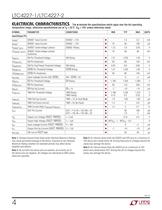
LTC4227-1/LTC4227-2 4 422712f E lectrical CharacteristicsThe l denotes the specifications which apply over the full operating temperature range, otherwise specifications are at TA = 25°C. VIN = 12V, unless otherwise noted. SYMBOL PARAMETER CONDITIONS MIN TYP MAX UNITS Input/Output Pin ISENSE + SENSE+ Input Current SENSE+ = 12V l 1.2 2.2 mA ISENSE – SENSE– Input Current SENSE– = 12V l 10 50 100 ìA VSENSE + (UVL) SENSE+ Undervoltage Lockout SENSE+ Rising l 1.75 1.9 2.05 V ÄVSENSE + (HYST) SENSE+ Undervoltage Lockout Hysteresis l 10 50 90 mV VON(TH) ON Pin Threshold Voltage ON Rising l 1.21...
Open the catalog to page 4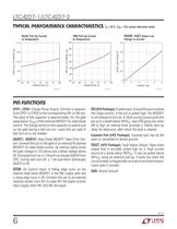
LTC4227-1/LTC4227-2 6 422712f HGATE Pull-Up Current vs Temperature TMR Pull-Up Current vs Temperature PWRGD, FAULT Output Low Voltage vs Current Typical Performance Characteristics TA = 25°C, VIN = 12V, unless otherwise noted. Pin Functions CPO1, CPO2: Charge Pump Output. Connect a capacitor from CPO1 or CPO2 to the corresponding IN1 or IN2 pin. The value of this capacitor is approximately 10× the gate capacitance (CISS) of the external MOSFET for ideal diode control. The charge stored on this capacitor is used to pull up the gate during a fast turn-on. Leave this pin open if fast turn-on...
Open the catalog to page 6
LTC4227-1/LTC4227-2 7 422712f Pin Functions HGATE: Hot Swap MOSFET Gate Drive Output. Connect this pin to the gate of the external N-channel MOSFET for Hot Swap control. An internal 10ìA current source charges the MOSFET gate. An internal clamp limits the gate voltage to 12V above and a diode voltage below OUT. During turn-off, a 300ìA pull-down discharges HGATE to ground. During an output short or INTVCC undervoltage lockout, a fast 200mA pull-down discharges HGATE to OUT. IN1, IN2: Positive Supply Input and MOSFET Gate Drive Return. Connect this pin to the power input side of the external...
Open the catalog to page 7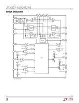
LTC4227-1/LTC4227-2 8 422712f Block Diagram + – + – A1 + – GA1 12V 12V HGATE OUT CPO1 DGATE1 ON CPO2 DGATE2 65mV IN1 SENSE+ SENSE– IN2 10ìA –+ 50mV ECB –+ 25mV 1.235V HGATE ON 0.6V 2.2V 10ìA INTVCC CP1 25mV –+ 100ìA INTVCC INTVCC 100ìA + – INTVCC –+ CHARGE PUMP 1 GATE DRIVER CHARGE PUMP 2 GA2 100ìA INTVCC 2ìA INTVCC INTVCC + – FAULT RESET CP2 CP3 + – 1.235V DGATE2 OFF CP4 + – 1.235V 0.2V CP5 + – CP6 + – 1.235V CARD PRESENCE DETECT LOGIC + – D2ON TMR *UFD PACKAGE ONLY EN* 10ìA 10ìA UV1 GND 422712 BD FAULT* PWRGD + – NC* EXPOSED PAD* 1.9V SENSE+ UV2 + – 5V LDO 12V
Open the catalog to page 8
LTC4227-1/LTC4227-2 9 422712f Operation The LTC4227 functions as an input supply diode-OR with inrush current limiting and overcurrent protection by controlling the external N-channel MOSFETs (MD1, MD2 and MH) on a supply path. This allows boards to be safely inserted and removed in systems with a backplane powered by redundant supplies. The LTC4227 has a single Hot Swap controller and two separate ideal diode controllers, each providing independent control for the two input supplies. When the LTC4227 is first powered up, the gates of the MOSFETs are all held low, keeping them off. As the...
Open the catalog to page 9All ADI catalogs and technical brochures
-
 LTC2068
30 Pages
-
 LTC6373
34 Pages
-
 ADL9006
16 Pages
-
 ADL8104
23 Pages
-
 AD4115
52 Pages
-
 ADUM7702
22 Pages
-
 AD7383
33 Pages
-
 AD7384
33 Pages
-
 AD4114
49 Pages
-
 ADUM7704
22 Pages
-
 AD7134
86 Pages
-
 LTspice IV
53 Pages
-
 New Products Catalog
43 Pages
-
 RF/IF Amplifiers
9 Pages
-
 SAR ADC Drivers
2 Pages
-
 SmartMesh Brochure
8 Pages
-
 INDUSTRIAL SIGNAL CHAIN
24 Pages
-
 AUTOMOTIVE ELECTRONIC SOLUTIONS
48 Pages
-
 Battery Management Solutions
32 Pages
-
 DC/DC uModule Power Products
32 Pages
-
 Wireless & RF Solution
36 Pages
-
 LT6656 - 1
18 Pages


Archived catalogs
-
 New Products Catalog
39 Pages
-
 Power Management for LEDs
24 Pages
-
 High Speed ADC Products Brochure
14 Pages


