- Catalogs
- Laird Connectivity
- BL54L15, BL54L10 Series
BL54L15, BL54L10 Series
1 /42Pages

BL54L15, BL54L10 Series
1 /42Pages
Catalog excerpts
Datasheet BL54L15, BL54L10 Series Version 1.9
Open the catalog to page 1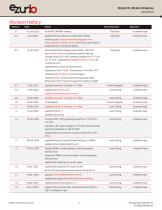
Revision History Version Date Notes Contributor(s) 10 June 2024 Initial PRELIMINARY release. 2 Oct 2024 Updated pin list names and notes below table1. Added section External Antenna Integration with BL54L15/BL54L10 MHF4 variant (453-00044/453-00226) Added section on Programmability. 24 Oct 2024 Removed Medium voltage mode (VDDM_nRF) from Specification Summary table and updated Normal voltage mode (VDD_nRF) operating range from 1.7V-2.6V to 1.7V-3.6V. Updated Block Diagram and Pin-out for 39 connection pins. Updated SCH symbol to remove pin40. Updated pin list in Table 1 (removed pin 40 VDDM_nRF)....
Open the catalog to page 2
© Copyright 2025 Ezurio All Rights Reserved
Open the catalog to page 3
© Copyright 2025 Ezurio All Rights Reserved
Open the catalog to page 4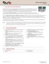
1 Overview and Key Features Experience a new pinnacle of performance, efficiency, and security with our new BL54L15 and BL54L10 series, built on Nordic Semiconductor's powerful nRF54L QFN silicon. Elevating what you know and love from the nRF52 series, this next generation redefines Bluetooth LE and 802.15.4 solutions. Unleashing enhanced processing power, expanded memory, and innovative peripherals, the BL54L15 is the ultimate choice for low power connectivity. Powered by Nordic's nRF54L15 and nRF54L10 SoC, our compact BL54L15 and BL54L10 modules deliver secure and robust Bluetooth LE and 802.15.4...
Open the catalog to page 5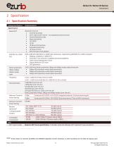
2 Specification2.1 Specification Summary Categories/Feature Notel Known Noise on channels 2432MHz and 2464MHz degrades receiver sensitivity, in which sensitivity are not within the typical value © Copyright 2025 Ezurio All Righ
Open the catalog to page 6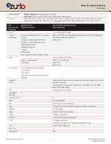
^uio mode compliant Modes of Operation: Disable, Sense, Activated Use Cases: Touch-to-Pair with NFC, NFC enabled Out-of-Band Pairing SeCurity Designed for PSA Certified Level 3 with Secure Boot, Secure Firmware Update, and Secure Storage. Integrated tamper sensors detect attacks and take action, and cryptographic accelerators are hardened against side-channel attacks. © Copyright 2025 Ezurio All Rights Reserved
Open the catalog to page 7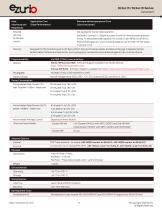
BL54L15 / BL54L10 SeriesDatasheet Host Application Core Software defined peripheral Core Interfaces and (High Performance) (ultra-low power) External optional 32.768 kHz crystal Not needed for normal radio operation. Optionally, connect +/-20ppm accuracy crystal for more accurate protocol timing. Fit associated load capacitor for crystal or use nRF54L15/nRF54L10 internal load capacitor, which is configurable as 4 pF to 18 pF in 0.5 pF steps on pins XL1, XL2. Designed for PSA Certified Level 3 with Secure Boot, Secure Firmware Update, and Secure Storage. Integrated tamper sensors detect attacks...
Open the catalog to page 8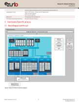
^uio Utilise the above development kits for projects planned with BL54L10. Development Tools Nordic nRFConnect - Android and iOS applications UART firmware upgrade Xbit Tools and utilities Bluetooth® Full Bluetooth SIG Declaration ID Optional External 32.768 kHz Crystal Figure 1: BL54L15/ BL54L10 HWblock diagram © Copyright 2025 Ezurio All Rights Reserved
Open the catalog to page 9
Figure 2: Top view - Schematic symbol for453-00001/453-00225BL54L15/L10 Module (Nordic nRF54L15/L10) - integrated PCB Trace Antenna variant or453-00044/453-00226MHF4 RF connector variant Pin Pin Name (red nRF54L15 nRF54L15/ nRF54L10 QFN48 Description Example usage # coloured pins for clock nRF54L10 Name SPIM SDI SPIS SDI UARTECTS General purpose I/O Trace data Trace General purpose I/O Trace data Trace Serial wire output (SWO) T race 5 SWDIO 25 SWDIO Serial Wire Debug IO for 6 SWDCLK 26 SWDCLK Serial Wire Debug clock input for debug and programming 7 NRESET 30 nRESET Pin RESET with internal pull-up...
Open the catalog to page 10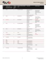
BL54L15 / BL54L10 SeriesDatasheet Pin Pin Name (red nRF54L15 nRF54L15/ nRF54L10 QFN48 Description # coloured pins for clock nRF54L10 Name Example usage 8 P2.02 13 P2.02/SPI.SDl/SDO General purpose I/O SPIM SDO SPIS SDO UARTETXD QSPI D0 Serial wire output (SWO) SPIM DCX UARTE RXD QSPI D3 SPIM SCK SPIS SCK QSPI SCK SPIM SDI SPIS SDI UARTE CTS QSPI D1 SPIM CS UARTE RTS QSPI CS TAMPC active shield 1 input Analog input TAMPC active shield 1 Analog input © Copyright 2025 Ezurio All Rights Reserved
Open the catalog to page 11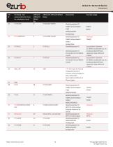
# coloured pins for clock nRF54L10 Name © Copyright 2025 Ezurio All Rights Reserved
Open the catalog to page 12
BL54L15 / BL54L10 SeriesDatasheetPin Pin Name (red nRF54L15 nRF54L15/ nRF54L10 QFN48 Description Example usage # coloured pins for clock nRF54L10 Name 34 P1.12/AIN5/CLK 40 P1.12/AIN5 General purpose I/O Clock pin TAMPC active shield 3 TAMPC input RADIO RADIO DFEGPIO Analog input TAMPC active shield 3 output RADIO DFEGPIO Analog input GRTC PWM output General purpose I/O Trace SPIM CS UARTERTS SPIM SCK SPIS SCK Trace clock Note2 Clock for serial interfaces or trace Note 3 Dedicated pins Note 4 SWDIO / SWCLK / nRESET / VDD / GND GPIO = General Input or Output (GPIO level voltage tracks VDD pin)....
Open the catalog to page 13
3.3 Electrical Specifications 3.3.1 Absolute Maximum Ratings Absolute maximum ratings are the extreme limits for supply voltage and voltages on digital and analogue pins of the module are listed below; exceeding these values causes permanent damage. Table 2: Absolute maximum ratings Supply Voltages Storage temperature MSL (Moisture Sensitivity Level) Flash Memory (Endurance) (Note 2) Flash Memory (Retention) Write/erase cycles years at TBD °C Absolute maximum Ratings Notes: Note 1 The absolute maximum rating for VDD pin (max) is 3.6 V for the BL54L15. Note 2 Wear levelling can be implemented...
Open the catalog to page 14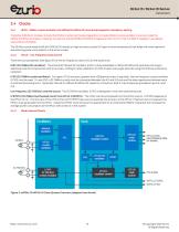
HFXO - 32MHz crystal oscillator and nRF54L15/nRF54L10 internal load capacitor mandatory setting The BL54L15/BL54L10 module contains the 32 MHz crystal, but the load capacitors to create 32MHz crystal oscillator circuit are inside the nRF54L15/nRF54L10 chipset. Customer can set the internal nRF54L15/nRF54L10 capacitors from 4 pF to 17 pF in 0.25pF if needed or use default value without changing. The 32 MHz crystal inside the BL54L15/BL54L10 module is a high accuracy crystal (±15 ppm at room temperature) that helps with radio operation and reducing power consumption in the active modes. 3.4.2 LFCLK...
Open the catalog to page 15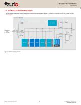
3.5 BL54L15/ BL54L10 Power Supply Normal voltage mode power supply mode is entered when the external supply voltage (1.7V-3.5V) is connected to both VDD_nRF pin (pin26). See Figure 4. External Power Figure 4: Normal Voltage Mode © Copyright 2025 Ezurio All Rights Reserved
Open the catalog to page 16All Laird Connectivity catalogs and technical brochures
 Aurawave AW100 Series
14 Pages
 SentriusTM BT610 I/O Sensor
3 Pages
- Display module
- Temperature probe
- Touch screen display panel
- Waterproof temperature sensor
- HMI
- HMI with touch screen
- Wireless gateway
- SoM
- IoT gateway
- Ethernet HMI
- Communication module
- USB HMI
- Omnidirectional antenna
- RS-232 HMI
- Industrial HMI
- Numeric display
- Compact gateway
- 7" display panel
- WLAN antenna
- Industrial system-on-module