 Website:
KoCoS Messtechnik AG
Catalog excerpts

KOCOS - THE TECHNOLOG Y GROUP | WHERE PRECISION MEET S QUALIT Y WATOM. . Wafer Topography Measurement KOCOS AUTOMATION
Open the catalog to page 1
WATOM Wafer edge and notch profile measurement The use of smaller and smaller patterns in the semiconductor industry calls for increasingly advanced materials of extremely high quality. In response to the steady improvements in the quality of wafers, KoCoS Automation has developed WATOM, a wafer edge and notch profile measurement tool which heralds a new era of extremely precise wafer geometry measurement. WATOM supports quality assurance throughout the wafer manufacturing process, starting at the very beginning and continuing on through to wafer reclaim. The WATOM Edge and Notch Wafer...
Open the catalog to page 3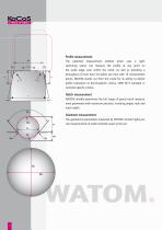
Profile measurement The patented measurement method which uses a light- sectioning sensor can measure the profile at any point on the wafer edge, even within the notch. As well as providing a throughput of more than 50 wafers per hour with 16 measurement points, WATOM stands out from the crowd for its ability to deliver profile evaluation to KoCoS-specific criteria, SEMI M73 standard or customer-specific criteria. Notch measurement WATOM reliably determines the full range of typical notch measurement parameters with maximum precision, including angles, radii and notch depth. Diameter...
Open the catalog to page 4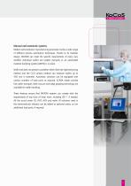
Manual and automatic systems Modern semiconductor manufacturing processes involve a wide range of different process automation techniques. Thanks to its modular design, WATOM can meet the specific requirements of every user, whether individual wafers are loaded manually or an automated material handling system (AMHS) is in place. Wafer size does not present a problem either. Both the light-sectioning method and the CCD camera method can measure wafers up to 450 mm in diameter. Automatic solutions can be equipped with various numbers of load ports as required. SCARA robots provide fast...
Open the catalog to page 5
WATOM T Small footprint and consistent accuracy The latest innovation from KoCoS adds a new tool to the WATOM product family. WATOM T is a compact, inexpensive alternative for applications that have no automation requirements and provides the same quality, process reliability and measurement precision as other WATOM systems. It is a reliable solution for space-saving integration in the production process and for sample test requirements. WATOM T is designed to accept two wafer sizes. Once a wafer has been placed manually on the transfer stage, it is loaded and the measurement runs...
Open the catalog to page 6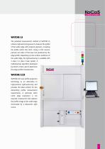
WATOM LS The patented measurement method of WATOM LS utilizes a light-sectioning sensor to measure the profile of the wafer edge with pinpoint precision, including the profile within the notch. Using a CCD camera, pictures are taken of the laser line produced by the edge profile. Depending on the surface conditions of the wafer edge, the light-sectioning is available with a class 2 or class 3 laser system. A mathematical algorithm developed by KoCoS is then used to determine the edge profile characteristics. WATOM CCD WATOM CCD uses profile projection technology as an alternative to...
Open the catalog to page 7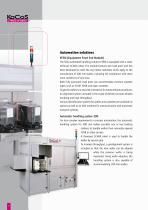
Automation solutions EFEM (Equipment Front End Module) The fully automated handling solution EFEM is equipped with a state-of-the-art SCARA robot. The module features two load ports and has been developed to meet the very latest standards which apply to the manufacture of 300 mm wafers, including full compliance with clean room conditions of any class. Both fully automatic load ports can accommodate common cassette types, such as FOUP, FOSB and open cassettes. To get the wafers to a required orientation for measurement procedures, an alignment system included in the scope of delivery...
Open the catalog to page 8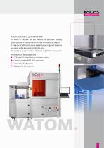
Automatic handling system 150/200 For wafers of 150 and 200 mm diameter the automatic handling system provides 4 loading stations without increasing the footprint. A three-axis SCARA robot ensures a wide motion range and maximum axis travel with a decreased interference area. The module is equipped with an alignment and identification system. All modules can be equipped with ■ OCR wafer ID readers for top or bottom reading ■ Carrier ID readers (BCR, RFID reader, etc.) ■ Vacuum handling systems ■ Edge grip handling systems
Open the catalog to page 9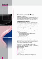
Measurement and evaluation features Large variety of materials Using highly precise handling solutions, the WATOM product family can accommodate many substrate materials such as silicon, germanium, gallium arsenide, gallium nitride, sapphire, glass, quartz, ceramics, etc. Three-dimensional notch edge profile Due to the latest developments in the KoCoS light-sectioning system, evaluation of the edge profile is possible within the whole notch area. Several profile measuring points inside the notch, including the edge profile of the notch ground, the wings and the radii, allow threedimensional...
Open the catalog to page 10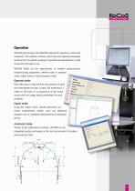
Operation WATOM systems rely on the WATOM software for operation, control and evaluation. This modular software, which has been specially developed by KoCoS for the specific purpose of geometrical measurement, is well structured and easy to use. WATOM fulfills all the requirements of modern semiconductor manufacturing equipment, whether used in operator mode, expert mode or fully automatic mode. Operator mode Very little input is required from the operator to start the measurement process. A pass/fail assessment is made on the basis of a comparison of the actual results with the target...
Open the catalog to page 11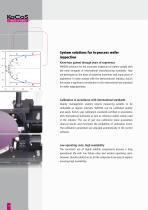
System solutions for in-process wafer inspection Know-how gained through years of experience WATOM solutions for the in-process inspection of wafers comply with the most stringent of international manufacturing standards. They are developed on the basis of extensive know-how and many years of experience. In close contact with the semiconductor industry, KoCoS has made a significant contribution to the international test standard for wafer edge geometry. Calibration in accordance with international standards Quality management systems require measuring systems to be calibrated at regular...
Open the catalog to page 12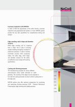
In-process inspection with WATOM In order to fulfil the requirements of the wafer industry, in-process inspection using appropriate test systems is a must. WATOM systems provide the very best possibilities for comprehensive testing and analysis. Edge rounding, notch shape and diameter variance Wafer edge rounding and its inspection have a major role to play in ensuring reliable handling throughout hundreds of production processes. In order to achieve nanometer accuracy when processing wafers, the wafer edge, notch shape and diameter variance for the whole circumference must comply with...
Open the catalog to page 13All KoCoS Messtechnik AG catalogs and technical brochures
-
OMCAT Series
12 Pages
-
3D inspection system
16 Pages
-
LOTOS LT
2 Pages
-
LOTOS
16 Pages
-
OMCAT
12 Pages
-
INDEC
2 Pages
-
ACTAS L Series
2 Pages
-
PROMET L100s
2 Pages
-
PROMET L10
2 Pages
-
PROMET R300
2 Pages
-
PROMET SE
2 Pages
-
ACTAS BTT 2.0
2 Pages
-
EPOS MC4
2 Pages
-
EPOS CV SERIES
2 Pages
-
EPOS 360
2 Pages
-
Circuit Breaker Testing
10 Pages
-
SHERLOG CRX 2032
2 Pages
-
SHERLOG CRX
2 Pages
-
EPPE RX
2 Pages
-
EPPE CX
2 Pages
-
EPPE PX
2 Pages
-
ACTAS P360+
2 Pages
-
ACTAS P260+
2 Pages
-
ARTES 600
2 Pages
-
ARTES 460 II
2 Pages
-
ARTES RC3
2 Pages
-
Circuit Breaker Testing
2 Pages
-
Fault Recorder Systems
14 Pages


