Catalog excerpts
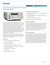
RF Vector Signal GeneratorsTSG4100A Series The TSG4100A Series RF Vector Signal Generator offers mid-range performance and up to 200 MHz modulation bandwidth at an entry-level RF signal generator price. They use a new technique to provide spurious free outputs with low phase noise (-113 dBc/Hz at 20 kHz offset from 1 GHz carrier) and extraordinary frequency resolution (1 |jHz at any frequency). The TSG4100A Series comes standard with analog modulation. Convenient, in-field software upgrades allow for easy transition from analog to more advanced vector and digital modulation capabilities, providing the most flexible configuration and best CAPEX protection. These instruments complement other leading mid-range RF test solutions from Tektronix, such as the USB-based RSA306 Spectrum Analyzer and MDO4000B and MDO3000 Mixed Domain Oscilloscopes. The TSG4100A Series instruments use an ovenized SC-cut oscillator (TSG410xA-M00 or E1 models) time-base, providing a 100 X improvement in stability (and a 100 X reduction in the in-close phase noise) compared to instruments that use a TCXO time-base. Key features • Analog and vector/digital signal generation capabilities • Dual baseband ARB generators • Analog modulation standard • Soft key upgrade to vector/digital modulation at very low cost • Digital modulation applications for GSM, EDGE, W-CDMA, APCO-25, DECT, NADC, PDC, and TETRA Key performance specifications • True DC to 2 GHz, 4 GHz or 6 GHz to support both analog and vector/ digital signal generation • Typical <±0.30 dB amplitude accuracy (0 dBm CW signal at 22 °C) from 10 MHz to 6 GHz • I/Q modulation inputs (400 MHz RF bandwidth) • ASK, FSK, MSK, PSK, QAM, VSB, and custom I/Q Analog modulation The Tektronix TSG4100A Series RF Vector Signal Generators offer a wide variety of modulation capabilities. Modes include amplitude modulation (AM), frequency modulation (FM), phase modulation ($>M), and pulse modulation. There is an internal modulation source as well as an external modulation input. The internal modulation source produces sine, ramp, saw, square, and noise waveforms. An external modulation signal may be applied to the rear panel modulation input. The internal modulation generator is available as an output on the rear panel. Vector modulation The TSG4100A Series builds on this performance by adding full support for vector signal modulation on RF carriers between 400 MHz and 6.0 GHz. It features a dual arbitrary waveform generator operating at 125 MHz for baseband signal generation. The generator has built-in support for the most common vector modulation schemes: ASK, QPSK, DQPSK, n/4 DQPSK, 8PSK, FSK, CPM, QAM (4 to 256), 8VSB, and 16VSB. It also includes built-in support for all the standard pulse shaping filters used in digital communications: raised cosine, root-raised cosine, Gaussian, rectangular, triangular, and more. Lastly, it provides direct support for the controlled injection of additive white Gaussian noise (AWGN) into the signal path. USB, GPIB, RS-232, and LAN interfaces 12 pounds (5.6 kg) 2U high and half standard rack width
Open the catalog to page 1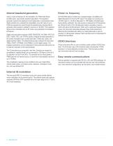
TSG4100A Series RF Vector Signal Generator Internal baseband generators Using a novel architecture for I/Q modulation, the TSG4100A Series provides quick, user-friendly waveform generation. The baseband generator supports the playback of pure digital data. It automatically maps digital symbols into a selected I/Q constellation at symbol rates of up to 6 MHz and passes the result through the selected pulse shaping filter to generate a final waveform updated in real time at 125 MHz. This baseband signal is then modulated onto an RF carrier using standard IQ modulation techniques. All TSG4100A...
Open the catalog to page 2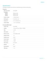
Specifications All specifications are guaranteed unless noted otherwise. All specifications apply to all models unless noted otherwise. Frequency BNC output, all models Frequency resolution Switching speed Frequency error Frequency stability Front panel BNC output Frequency range Offset resolution Maximum excursion Amplitude resolution Amplitude accuracy Harmonics, typical Spurious, typical Output coupling Reverse protection VSWR, typical
Open the catalog to page 3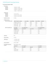
Front panel N-type output Power output TSG4102A +16.5 dBm to -110 dBm Voltage output TSG4102A 1.5 Vrms to 0.7Vrms
Open the catalog to page 4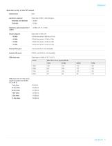
Spectral purity of the RF output Subharmonics None Harmonics, maximum Output level <0 dBm, 1 GHz CW signal Harmonics, typical (output level < < -35 dBc, CW , Fc < 2 GHz Spurious (typical) Output level -10 dBm, CW SSB phase noise Output level is +5 dBm at 18 °C to 28 °C. SSB phase noise at 1 GHz carrier, maximum (output level +5 dBm, 5 C to 40 C) 1 kHz offset -95 dBc/Hz 10 kHz offset 20 kHz offset 1 MHz offset 2 GHz offset >3 GHz offset -106 dBc/Hz -107 dBc/Hz -120 dBc/Hz -118 dBc/Hz -120 dBc/Hz
Open the catalog to page 5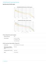
TSG4100A Series RF Vector Signal GeneratorSpectral purity of the RF outputPhase setting (front panel outputs) Maximum phase step ±360° Oscillator type Oven-controlled, 3rd OT, SC-cut crystal Initial accuracy at calibration <±0.02 ppm (20 minute warm-up, at 18 °C to 28 °C) Temperature drift (0 °C to 40 °C) <±0.003 ppm
Open the catalog to page 6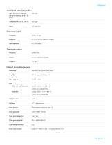
Datasheet VCXO time base (Option M01) Initial accuracy at calibration (20 minute warm-up, at 18 ºC to 28 ºC) Time-base input Frequency Input impedance Time-base output Frequency Internal modulation source Waveforms Sine, ramp, saw, square, pulse, noise Ramp linearity Rate resolution Rate error Noise function White Gaussian noise (rms = dev / 5) Noise bandwidth Pulse generator period Pulse generator width Pulse timing resolution Pulse noise function Length 2N-1 PRBS 5 ≤ N ≤ 32, bit period 100
Open the catalog to page 7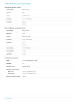
Connector type BNC (rear panel) Scale factor ±1 V for ± full deviation Connector type Scale factor Input coupling Pulse Threshold Input Offset BNC (rear panel) 100 kQ AM, FM, $M, Pulse ±1 V for ± full deviation Low = 0 V Hi = 3.3 V DC or 4 Hz High-pass +1 VDC < 500 gV Amplitude modulation Range 0 to 100% (decreases above +7 dBm) Modulation source Internal or external Modulation distortion, typical BNC output <1 % (fc < 62.5 MHz, fm = 1 kHz) Modulation bandwidth (external) >100 kHz
Open the catalog to page 8All Keithley Instruments catalogs and technical brochures
-
6220-6221
5 Pages
-
6482
3 Pages
-
2520
8 Pages
-
2606B
13 Pages
-
2601B
20 Pages
-
AFG1000 Series
13 Pages
-
AFG31000 Series Datasheet
22 Pages
-
2182A Nanovoltmeter
6 Pages
-
6 Series B MSO
69 Pages
-
Isolated Measurement Systems
8 Pages
-
TBS1000B-EDU Series
14 Pages
-
3 Series MDO
36 Pages
-
4 Series MSO
40 Pages
-
2461-EC Graphical Potentiostat
16 Pages
-
2460-EC Graphical Potentiostats
15 Pages
-
2450-EC Graphical Potentiostat
15 Pages
-
4200A-SCS Parameter Analyzer
45 Pages
-
MDO4000C Series Datasheet
43 Pages
-
RTPA2A
6 Pages
-
TPA-N-PRE Datasheet
4 Pages
-
DPO4PWR·MDO3PWR Datasheet
6 Pages
-
DPO4LMT/MDO3LMT Datasheet
6 Pages
-
DPO7000 Series Datasheet
28 Pages
-
SourceXpress® Datasheet
4 Pages
-
10G-KR Datasheet
8 Pages
-
DPO70000SX Series Datasheet
46 Pages
-
AWG4000 Series Datasheet
20 Pages
-
TLA6400 Series Datasheet
14 Pages
-
Potentiostats 2450-EC
8 Pages
-
4200-SCS
16 Pages
-
2013 Keithley product catalog
403 Pages
-
Nanotechnology Measurement
13 Pages
-
Semiconductor Device Test
11 Pages
-
Series 2400 SourceMeter®Family
16 Pages
Archived catalogs
-
8 Series Sampling Oscilloscope
14 Pages
-
Multimeter/Switch System
1 Pages


