

Polar3TM Power MOSFETs

Polar3TM Power MOSFETs
The Polar3TM Power MOSFET family is a new addition to IXYS' high-performance Polar-Series, utilizing the proprietary Polar3TM Technology Platform. These devices offer an optimized combination of low on-state resistance (Rdson) and gate charge (Qg), achieving a Figure of Merit (FOM) as low as 9.6 ΩnC. Key features include low thermal resistances, dynamic dV/dt ratings, high power dissipation, and high avalanche energy capabilities, making them suitable for high-voltage conversion systems.
Specifications
The Polar3TM family is available in 500V and 600V grades. The 500V devices have drain current ratings from 8A to 132A, while the 600V devices range from 4A to 110A. These devices feature low on-resistances (as low as 39mΩ) and low gate charge values (as low as 6.9nC), resulting in reduced power consumption. Compared to previous generations, they offer up to a 12% reduction in on-state resistance, 14% reduction in gate charge, and a 20% increase in maximum power dissipation.
Applications
These MOSFETs are ideal for high-speed switching applications such as switch mode power supplies (SMPS), uninterruptible power supplies (UPS), power factor correction circuits, motor drives, lamp ballasts, laser drivers, DC-DC converters, battery chargers, solar inverters, and robotic and servo controls.
Benefits
The Polar3TM MOSFETs provide high power density, reduced conduction and switching losses, enable high-speed switching, and promote the use of smaller passive components. They also allow for simpler and more economical gate drive solutions, cooler device operation, system miniaturization, increased device ruggedness, and easy mounting.
Features
Key features include low Rdson, low Qg, dynamic dV/dt ratings, avalanche rating, high power dissipation, low thermal resistance, fast intrinsic rectifier, low gate drive power requirements, and low package inductance.
Figures and Circuit Descriptions
Figures illustrate various circuit applications such as lamp ballast, telecom SMPS, and battery charger circuits, highlighting the use of Polar3TM HiPerFETTM Power MOSFETs for efficient and robust power switching duties.
Catalog excerpts
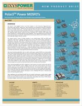
Polar3TM Power MOSFETs Next Generation Of Energy-ecient And Reliable Power-switching Solutions OVERVIEW The Polar3TM Power MOSFET family is the latest addition to IXYS’ benchmark high-performance Polar-Series Power MOSFET product line. These new devices are manufactured using IXYS’ proprietary Polar3TM Technology Platform, yielding new and improved devices that feature an optimized combination of low on-state resistance (Rdson) and gate charge (Qg). The end result is a device that achieves a Figure of Merit (FOM) performance index (device on-resistance multiplied by gate charge) as low as 9.6 ΩnC. Additional device features include low thermal resistances (RthJC), dynamic dV/dt ratings, high power dissipation (Pd), and high avalanche energy capabilities. These outstanding electrical and thermal device characteristics are essential for implementing improved power eciency and reliability in today’s demanding high-voltage conversion systems. The featured Polar3TM family is initially available in two voltage grades; 500V and 600V grade respectively. 500V Polar3TM oerings will include drain current (Id @ Tc=25ºC) ratings of 8Amperes to 132Amperes. Conversely, 600V Polar3TM oerings will have drain current (Id @ Tc=25ºC) ratings of 4Amperes to 110 Amperes. These devices feature low on-resistances (as low as 39mΩ) while delivering low gate charge values (as low as 6.9nC). The combined low conduction and switching losses resulted in a signicant reduction in the overall power consumption of the device. In comparison to previous Polar-Series generations (PolarP2 HiPerFETTM), these new Polar3 HiPerFETs demonstrate up to a 12 percent reduction in on-state resistance (Rdson), 14 percent reduction in gate charge (Qg) and as high as 20 percent increase in maximum power dissipation (Pd). Lower thermal resistances are also achieved due to reduced chip thicknesses, increasing total power density of the device. High speed switching applications such as switch mode power supplies (SMPS) and uninterruptible power supplies (UPS) will greatly benet from the low total gate charge and gate drain charge (Qg=6.9nC, Qgd=2.8nC, Vgs@10V) characteristics of these devices. The low total gate charge and gate drain charge characteristic allows designers the ability to boost power conversion eciency through the use of high-speed switching and to promote the use of smaller passive components, thus freeing up additional PCB real-estate and reducing the cost of bulky passive components. In additional, the low total gate charge reduces the amount of gate drive power requirement (Gate Drive Power = QG x VGS x FSW) needed for the Power MOSFET to fully conduct. Since these devices require less gate drive power, simple economical gate drive solutions can be implemented, further reducing cost and complexity. Type X PLUS247 Type H TO-247 Type K TO-264 Other applications that will greatly benet from the superior performance, energy savings, rugged design, and cost-eectiveness of these new 3rd generation Polar-Series Power MOSFETs include applications such as power factor correction circuits, motor drives, lamp ballasts, laser drivers, DC-DC converters, battery chargers, solar inverters, robotic and servo control. Low Rdson Low Qg Dynamic dV/dt ratings Avalanche Rated High power dissipation (Pd) Low Thermal Resistance (Rthjc) Fast intrinsic rectier Low gate drive power requirements Low package inductance BENEFITS High power density Reduces conduction and switching losses Enables high-speed switching Promotes use of smaller passive components Promotes use of simple economical gate drive solutions Cooler device operation Enables system miniaturization Increased device ruggedness Easy to mount Power switching capabilities and device ruggedness of these devices are further enhanced through the utilization of IXYS’ HiPerFETTM process, yielding a device with a fast intrinsic diode for low reverse recovery charge (Qrr) and improved turn-o dV/dt immunity. The enhanced dV/dt ratings of these devices oer signicant safety margins for the stresses encountered in high-voltage switching applications. Furthermore, these new devices eliminate the need for discrete anti-parallel high voltage diodes used in conventional designs, thereby reducing part count, simplifying PCB layouts, reducing overall losses and improving power density. APPLICATIONS Switch Mode Power Supplies Uninterruptible Power Supplies Power Factor Correction Circuits DC-DC converters Laser Drivers Battery Chargers AC and DC Motor Drives Robotics and Servo Controls Solar Inverters Lamp Ballasts
Open the catalog to page 1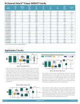
N-Channel Polar3TM Power MOSFET Family Part Number Package Style (1) Place holder in part number for package designator Module/Component Application Color Code Legend M1 DC-DC Converter MOSFET Driver DC-DC Converter Figure 1: Lamp Ballast Circuit MOSFET Driver Figure 1 illustrates a basic uorescent lamp ballast circuit. This electronic lamp ballast circuit topology consists of a primary rectier, power factor correction circuit, control Figure 2: 48V Telecom SMPS Circuit unit (DC-DC Converter, MCU, and Gate Driver), half-bridge inverter and a resonant output stage. An AC power source is converted...
Open the catalog to page 2All IXYS catalogs and technical brochures
 600V XPT IGBTs
2 Pages
 1200V XPT? IGBTs
2 Pages
 650V XPT? Trench IGBTs
2 Pages
 4500V POWER MOSFETs
2 Pages
 IXYS 2013
232 Pages
 BODO'S POWER SYSTEMS®
4 Pages
 IXYS News
6 Pages






Archived catalogs
 MICROCONTROLLERS Z8F0223QB005EG
245 Pages
 Selector guide
220 Pages
 IXYS RF Switch Mode MOSFET
2 Pages
 Breakover Diodes
8 Pages
 HiPerFETTM Power MOSFET
4 Pages
 NPT3 IGBT
4 Pages


- Switching relay
- Technology switch
- Multipole switch
- Generator
- Transistor module
- Solid state relay
- Touch switch
- DC solid state relay
- MOSFET transistor
- Bipolar transistor
- Microcontroller
- Digital generator
- Printed circuit board solid state relay
- IGBT transistor
- Analog microcontroller
- General purpose microcontroller
- Substrate
- DC output solid state relay
- Programmable microcontroller
- Radio-frequency switch