High Voltage, High Gain BIMOSFETTM Monolithic Bipolar MOS Transistor
1 /7Pages

High Voltage, High Gain BIMOSFETTM Monolithic Bipolar MOS Transistor
1 /7Pages
Catalog excerpts

Preliminary Technical Information High Voltage, High Gain BIMOSFET™ Monolithic Bipolar MOS Transistor (Electrically Isolated Tab) Symbol Test Conditions Maximum Ratings Vces Tc = 25°C to 150°C SSOA (RBSOA) P„ Vge = 15V, Tvj = 125°C, Rg = 20Q Clamped Inductive Load TC = 25°C 1.6mm (0.062 in.) from Case for 10s Plastic Body for 10 seconds Mounting Force 50/60Hz, 1 Minute Features • Silicon Chip on Direct-Copper Bond (DCB) Substrate • Isolated Mounting Surface • 4000V~ Electrical Isolation • High Blocking Voltage • High Peak Current Capability • Low Saturation Voltage • Low Gate Drive Requirement • High Power Density Symbol Test Conditions Characteristic Values Applications • Switch-Mode and Resonant-Mode Power Supplies • Capacitor Discharge Circuits © 2012 IXYS CORPORATION, All Rights Reserved
Open the catalog to page 1
Symbol Test Conditions Characteristic Values Notes: 1. Pulse test, t < 300|is, duty cycle, d < 2%. 2. Device must be heatsunk for high temperature leakage current measurements to avoid thermal runaway. PRELIMINARY TECHNICAL INFORMATION The product presented herein is under development. The Technical Specifications offered are derived from data gathered during objective characterizations of preliminary engineering lots; but also may yet contain some information supplied during a pre-production design evaluation. IXYS reserves the right to change limits, test conditions, and dimensions without...
Open the catalog to page 2
© 2012 IXYS CORPORATION, All Rights Reserved
Open the catalog to page 3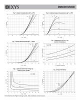
Fig. 2. Extended Output Characteristics @ T J = 25ºC 240 Fig. 4. Dependence of VCE(sat) on Junction Temperature VCE(sat) - Normalized Fig. 5. Collector-to-Emitter Voltage vs. Gate-to-Emitter Voltage IXYS Reserves the Right to Change Limits, Test Conditions and Dimensions.
Open the catalog to page 4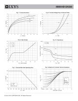
MMIX4B12N300 Fig. 8. Forward Voltage Drop of Intrinsic Diode Capacitance - PicoFarads Fig. 12. Maximum Transient Thermal Impedance Fig. 11. Reverse-Bias Safe Operating Area © 2012 IXYS CORPORATION, All Rights Reserved Pulse Width - Seconds
Open the catalog to page 5
MMIX4B12N300 Fig. 14. Resistive Turn-on Rise Time vs. Collector Current Fig. 13. Resistive Turn-on Rise Time vs. Junction Temperature 600 Fig. 18. Resistive Turn-off Switching Times vs. Gate Resistance Fig. 17. Resistive Turn-off Switching Times vs. Collector Current Fig. 16. Resistive Turn-off Switching Times vs. Junction Temperature Fig. 15. Resistive Turn-on Switching Times vs. Gate Resistance 700 IXYS Reserves the Right to Change Limits, Test Conditions and Dimensions.
Open the catalog to page 6
Disclaimer Notice - Information furnished is believed to be accurate and reliable. However, users should independently evaluate the suitability of and test each product selected for their own applications. Littelfuse products are not designed for, and may not be used in, all applications. Read complete Disclaimer Notice at www.littelfuse.com/disclaimer-electronics.
Open the catalog to page 7All IXYS catalogs and technical brochures
 Polar3TM Power MOSFETs
2 Pages
 600V XPT IGBTs
2 Pages
 1200V XPT? IGBTs
2 Pages
 650V XPT? Trench IGBTs
2 Pages
 4500V POWER MOSFETs
2 Pages
 IXYS 2013
232 Pages
 BODO'S POWER SYSTEMS®
4 Pages
 IXYS News
6 Pages


Archived catalogs
 MICROCONTROLLERS Z8F0223QB005EG
245 Pages
 Selector guide
220 Pages
 IXYS RF Switch Mode MOSFET
2 Pages
 Breakover Diodes
8 Pages
 HiPerFETTM Power MOSFET
4 Pages
 NPT3 IGBT
4 Pages


- Technology switch
- Generator
- Multipole switch
- Touch switch
- MOSFET transistor
- Bipolar transistor
- Microcontroller
- Digital generator
- IGBT transistor
- Analog microcontroller
- General purpose microcontroller
- Sensitive switch
- Programmable microcontroller
- Radio-frequency switch
- ADC microcontroller
- Semiconductor switch
- Photovoltaic solar cell
- Delay generator