

Mobile 3rd Gen Intel® Core? Processor Family: Datasheet, Vol. 1

Mobile 3rd Gen Intel® Core? Processor Family: Datasheet, Vol. 1
This document is a datasheet for the Mobile 3rd Generation Intel® Core™, Pentium®, and Celeron® Processor Families. It provides detailed information on processor features, interfaces, power management, and supported technologies.
The datasheet outlines supported technologies such as Intel® Virtualization Technology, Intel® Trusted Execution Technology, and Intel® Turbo Boost Technology. It also covers system memory support, PCI Express, Direct Media Interface (DMI), and processor graphics.
The document details various interfaces including system memory interface, PCI Express interface, and Direct Media Interface (DMI). It explains the architecture, configuration mechanisms, and compatibility assumptions for these interfaces.
Key technologies discussed include Intel® Virtualization Technology, Intel® Trusted Execution Technology, Intel® Hyper-Threading Technology, and Intel® Turbo Boost Technology. The document also covers security and cryptography technologies such as Intel® AES-NI and RDRAND instruction.
The datasheet provides information on power management support for processor cores, system, memory controller, PCI Express, and processor graphics controller. It also discusses thermal management support.
This section defines the different SKUs within the processor family, detailing their specifications and compatibility.
Information on processor packaging and compatibility with other components is provided, ensuring designers understand the requirements for integration.
The document includes a glossary of terms and references to related documents for further information.
The processors offer four or two execution cores, with a 32-KB instruction and data first-level cache (L1) for each core, a 256-KB shared second-level cache (L2), and up to 8-MB shared third-level cache (L3). Supported technologies include Intel® Virtualization Technology, Intel® Active Management Technology, Intel® Trusted Execution Technology, Intel® Turbo Boost Technology, and more.
The processors support two channels of DDR3/DDR3L/DDR3L-RS memory with a maximum of two DIMMs per channel. They support single-channel and dual-channel memory organization modes, with a theoretical maximum memory bandwidth of 21.3 GB/s in dual-channel mode with DDR3 1333 MT/s and 25.6 GB/s with DDR3 1600 MT/s.
The PCI Express* lanes are compliant with the PCI Express Base Specification, Revision 3.0, supporting 8.0 GT/s transfer speeds. The interface supports configurations such as 1x8, 2x4, and 1x16 for graphics and I/O, with a maximum theoretical bandwidth of 16 GB/s in each direction simultaneously for x16 Gen 3.
The document outlines the specifications for the Mobile 3rd Generation Intel® Core™ Processor Family, Intel® Pentium® Processor Family, and Intel® Celeron® Processor Family. It includes details on supported interfaces, memory technologies, and PCI Express capabilities.
The Integrated Memory Controller (IMC) supports DDR3, DDR3L, and DDR3L-RS protocols with two independent 64-bit channels. It supports up to two unbuffered non-ECC DDR3 DIMMs per channel, allowing up to four device ranks per channel. The processor supports JEDEC-approved memory modules and devices, with specific data transfer rates and DRAM device technologies.
The IMC supports various speed bins, CAS Write Latency (CWL), and command signal mode timings. The document provides detailed tables on supported DDR3/DDR3L/DDR3L-RS SO-DIMM module configurations and maximum memory sizes per DIMM.
The IMC supports single-channel and dual-channel modes, including Intel® Flex Memory Technology Mode, which divides memory into symmetric and asymmetric zones. Dual-Channel Symmetric Mode provides maximum performance by interleaving addresses between channels.
Intel® Fast Memory Access (Intel® FMA) includes Just-in-Time Command Scheduling, Command Overlap, and Out-of-Order Scheduling to optimize bandwidth and reduce latency. Data Scrambling is used to minimize the impact of excessive di/dt on the platform DDR3 VRs.
The processor supports one external x16 PCI Express Graphics Device, with Gen 3 speed capabilities. The PCI Express architecture is divided into Transaction, Data Link, and Physical Layers, each responsible for different aspects of packet communication and error management.
The PCI Express link is mapped through a PCI-to-PCI bridge structure, extending the configuration space to 4096 bytes per device/function.
Intel VT allows a single system to function as multiple independent systems, enabling multiple operating systems to run simultaneously. It includes Intel VT-x for hardware support in processors and Intel VT-d for I/O virtualization. Key features of Intel VT-x include Extended Page Tables (EPT), Virtual Processor IDs (VPID), Guest Preemption Timer, and Descriptor-Table Exiting. Intel VT-d focuses on domain-based isolation and hardware-based virtualization, supporting features like DMA remap engines and interrupt remapping.
Intel TXT enhances platform security by providing a measured and controlled launch of system software, establishing a protected environment. It uses Safer Mode Extensions (SMX) for measured/verified launch and protection mechanisms to prevent unauthorized modifications.
Intel HT allows an execution core to function as two logical processors, sharing some resources but maintaining separate architectural states. It requires BIOS and operating system support and is recommended for use with specific Windows versions.
This technology allows processors to run faster than their rated frequency when power and thermal conditions permit, enhancing performance for both multi-threaded and single-threaded workloads. Turbo Boost is dynamic and depends on factors like core activity, power consumption, and temperature.
Intel AVX extends the Intel instruction set to 256-bit vectors, improving performance for applications requiring vector floating-point operations. It includes new instructions for better data management and processing efficiency.
Intel AES-NI provides fast and secure data encryption and decryption using SIMD instructions, supporting a wide range of cryptographic applications. The PCLMULQDQ instruction supports carry-less multiplication, essential for cryptographic processing.
The document discusses several advanced features and specifications of Intel processors, focusing on cryptographic systems, random number generation, and interrupt delivery mechanisms. Key features include the RDRAND instruction for high-quality random number generation compliant with ANSI X9.82 and NIST SP 800-90 standards, and the x2APIC architecture which enhances processor addressability and interrupt delivery efficiency.
The x2APIC architecture extends the xAPIC architecture, providing backward compatibility and forward extensibility. It supports increased processor addressability with a 32-bit physical and logical xAPIC ID field, allowing for a larger number of processors to be addressed. The architecture also introduces a more efficient MSR interface for accessing APIC registers, enhancing interrupt delivery performance.
This feature enhances system protection by blocking malicious software attacks from user mode code when the system operates at the highest privilege level, thus safeguarding against viruses and unwanted code.
PAIR technology optimizes power-performance by routing interrupts based on core sleep states, enhancing energy savings and performance in high interrupt scenarios.
The document outlines various power management states supported by the processor, including ACPI states, processor core states, and integrated memory controller states. It details the transition between different power states, such as active, idle, and low-power states, and the role of Enhanced Intel SpeedStep Technology in optimizing processor frequency and voltage for performance and efficiency.
The processor supports multiple ACPI states, including full on, suspend-to-RAM, suspend-to-disk, and soft off states. Processor core states range from active mode (C0) to various low-power idle states (C1, C1E, C3, C6, C7), each offering different levels of power savings and latency.
This technology allows for multiple frequency and voltage points, optimizing performance and power efficiency. It supports software-controlled frequency selection and ensures glitch-free transitions between power states.
Low-power idle states (C-states) are used to save power when the processor is idle. Higher C-states offer more power savings but have longer entry and exit latencies. The document emphasizes the importance of enabling all low-power idle states for long-term reliability.
1. Core C3 State: Threads enter C3 by P_LVL2 I/O read or MWAIT(C3). Caches are flushed to L3, and core clocks stop.
2. Core C6 State: Threads enter C6 by P_LVL3 I/O read or MWAIT(C6). Architectural state is saved to SRAM, and voltage is reduced to zero.
3. Core C7 State: Similar to C6, but the last core entering C7 flushes L3 cache. Supports C7s substate for efficient L3 cache flushing.
4. C-State Auto-Demotion: Automatically demotes deeper C-states to C3 or C1 based on residency history to improve battery life.
1. Package C0: Normal operating state. At least one core is active.
2. Package C1/C1E: No additional power reduction in C1. C1E reduces core clock frequency and voltage.
3. Package C3: Entered when at least one core is in C3. L3 cache remains valid.
4. Package C6: Entered when at least one core is in C6. Core voltages are reduced to zero, but L3 cache remains powered.
5. Package C7: Entered when all cores are in C7 and L3 cache is flushed. Maximizes power savings.
1. Disabling Unused System Memory Outputs: Unused signals are tri-stated to reduce power consumption and signal quality issues.
2. DRAM Power Management: Supports various power-down modes (APD, PPD, DLL-off) to save power based on DDR configuration.
3. Conditional Self-Refresh: Memory enters self-refresh in low-power states (C3, C6, C7) if no memory requests are pending.
4. Dynamic Power Down: Memory ranks are powered down based on idle conditions to save power.
The document outlines various power management techniques for DRAM, DDR, PCI Express, DMI, and graphics components in a processor. It emphasizes dynamic power down modes, electrical power gating, and specific technologies for graphics power management.
The processor can dynamically put DRAM devices into power down states, either active or precharge, with precharge offering greater power savings. Dynamic power down involves powering up all ranks before a refresh cycle and powering down afterward.
DDR I/O supports on-die EPG during normal operation, allowing the processor to transition in and out of EPG mode as needed without external signals. During EPG, most DDR IO logic is powered down except for physical control registers.
Active power management is supported using L0s and L1 states, with inputs and outputs disabled in L2/L3 Ready state. Disabling ASPM may increase power consumption.
Several technologies are discussed, including Intel Rapid Memory Power Management (RMPM), Graphics Performance Modulation Technology (GPMT), and Dynamic Frequency Technology. These technologies aim to optimize power usage by adjusting memory states, render frequencies, and voltages based on workload and system conditions.
The thermal solution must ensure the processor remains below the maximum junction temperature and conforms to system constraints. Intel Turbo Boost Technology allows cores to run faster than baseline frequency, utilizing available thermal capacitance. Power monitoring and control are crucial for maintaining performance within thermal limits.
Turbo Boost Technology involves power monitoring and control to optimize performance within thermal and power constraints. It uses architectural counters for power estimation and allows customization through various control settings accessible via MSR, MMIO, or PECI interfaces.
The document outlines the thermal management mechanisms for Intel processors, focusing on the Intel Turbo Boost operation and the Adaptive Thermal Monitor. It details how these systems manage processor temperature to prevent overheating and maintain performance.
The processor uses a temperature offset mechanism to manage Turbo Boost operation. An offset can be set in the TEMPERATURE_TARGET MSR to adjust the throttling point, which should be lower than other protection mechanisms like ACPI trip points.
Upon activation of the Thermal Control Circuit (TCC), the processor dynamically reduces power by adjusting frequency and voltage. This process is automatic and does not require BIOS intervention. Voltage transitions precede frequency changes during upward transitions and vice versa during downward transitions. The voltage regulator must support dynamic VID steps for this method.
If frequency/voltage adjustments are insufficient, clock modulation is used, turning clocks on and off at a specific duty cycle. This cycle is dynamically adjusted based on need and is independent of processor frequency.
Each processor core has a DTS for accurate temperature monitoring. The DTS provides a relative temperature reading, which software must convert to an absolute temperature. The PECI interface can be used for average temperature readings, beneficial for fan speed control.
The PROCHOT# signal is asserted when the processor reaches its maximum operating temperature. It can be configured as bi-directional to protect other components. The signal remains active until the temperature drops below the thermal trip point.
This mode allows system software to reduce power consumption via clock modulation, independent of processor temperature. It can be used alongside the Adaptive Thermal Monitor but is overridden by the TCC's factory settings.
The integrated memory controller provides thermal protection for memory DIMMs through bandwidth throttling, based on temperature readings from physical sensors or estimated temperatures.
PECI is used for communication between the processor and platform for thermal management, allowing for temperature monitoring and control.
1. SKTOCC# / PROC_DETECT#: This signal is used to determine if the processor is present by being pulled down directly to the ground on the processor package.
2. PROC_SELECT#: Indicates the processor family. High output for 2nd Generation Intel® Core™ processors and low for 3rd Generation Intel® Core™, Pentium®, and Celeron® processors.
3. VCCIO_SEL: Initially intended for I/O voltage selection, but now should not be used as the voltage is the same across specified processor families.
1. VCC: Processor core power rail.
2. VCCIO: Processor power for I/O.
3. VDDQ: Processor I/O supply voltage for DDR3.
4. VAXG: Graphics core power supply.
5. VCCPLL: Provides isolated power for internal processor PLLs.
6. VCCSA: System Agent power supply.
These signals provide isolated, low impedance connections to various processor voltages and grounds, allowing for voltage sensing or measurement near the silicon.
1. VSS: Processor ground node.
2. VSS_NCTF: Signals for package mechanical reliability.
3. DC_TEST_xx#: Signals for solder joint reliability.
Details the pull-up and pull-down resistor values for various signals, ensuring proper signal integrity and functionality.
1. Power and Ground Pins: All power pins must be connected to their respective processor power planes, and all VSS pins to the system ground plane. Multiple power and ground planes are recommended to reduce I*R drop.
2. Decoupling Guidelines: Proper output decoupling is essential to maintain voltage specifications and prevent timing violations or reduced processor lifetime.
3. Voltage Identification (VID): The processor uses a serial VID interface for automatic voltage selection, with specific VID values set during manufacturing. The voltage regulator must comply with these VID values to ensure proper operation.
The document provides detailed electrical specifications for Intel processors, focusing on voltage identification, signal groups, and storage conditions.
The VID is crucial for configuring the processor's voltage levels. The VCCSA is set by the processor output pins VCCSA_VID[1:0], with default logic states and dynamic changes for power optimization in Ultra products.
Guidelines are provided for handling reserved signals, emphasizing that improper connections can lead to malfunction or incompatibility. Unused inputs should be connected to appropriate signal levels, while unused outputs may remain unconnected.
Signals are categorized by buffer type and characteristics, with specific termination requirements. Differential signals and selected DDR3 signals have On-Die Termination (ODT) resistors.
Intel recommends the processor be first in the TAP chain, supporting IEEE 1149.1-2001 and IEEE 1149.6-2003 standards. Translation buffers may be necessary for voltage compatibility.
Storage conditions prior to board attachment are specified, with temperature and humidity limits to prevent physical damage. Adherence to JEDEC standards is recommended for reliability.
DC specifications are defined at processor pins, with tables listing voltage and current specifications for various components like the processor core, memory controller, and system agent. Long-term reliability is contingent on adhering to specified limits.
- Table 7-1: IMVP7 Voltage Identification Definition
- Table 7-2: VCCSA_VID Configuration
- Table 7-3: Signal Groups
- Table 7-4: Storage Condition Ratings
- Table 7-5: Processor Core DC Voltage and Current Specifications
- Table 7-6: Processor Uncore Supply DC Voltage and Current Specifications
- Table 7-7: Memory Controller Supply DC Voltage and Current Specifications
- Table 7-8: System Agent Supply DC Voltage and Current Specifications
- Processor PLL (VCCPLL): The supply voltage is specified at 1.8V with a tolerance of ±5%. The maximum current for the VCCPLL rail is 1.2A.
- Processor Graphics (VAXG): The active VID range varies from 0.65V to 1.35V depending on the configuration. The maximum current for the graphics rail ranges from 18A to 46A, depending on the specific processor model.
- DDR3/DDR3L Signal Group: Specifications include input and output voltage levels, pull-up and pull-down resistances, and on-die termination resistances.
This document provides detailed information about the processor pin, signal, and package specifications for various processor models, including BGA1023 and rPGA988B. It includes a comprehensive list of ball names, numbers, buffer types, and directions, which are crucial for understanding the processor's connectivity and functionality.
- Ball List: The document lists the processor balls by name, number, buffer type, and direction. This includes DDR3 I/O, power (PWR), ground (GND), and analog signals. The list is essential for hardware engineers to design and debug processor connections.
- Mechanical Package Information: Figures 8-6 to 8-14 illustrate the mechanical packages for different processor configurations, such as 2C/GT1, 2C/GT2, and 4C/GT2. These diagrams are vital for understanding the physical layout and dimensions of the processors.
- DDR Data Swizzling: This section explains the DDR data pin swizzling technique used to enhance memory performance and timing. It highlights the importance of considering swizzling during debugging and provides a swizzling table for reference.
- DDR3 I/O and Power Connections: Detailed pin assignments for DDR3 I/O and power connections are provided, which are crucial for ensuring proper electrical connections and signal integrity.
- Debugging Considerations: The document emphasizes the need to account for DDR data swizzling during debugging to ensure accurate memory analysis.
This datasheet is an essential resource for engineers involved in processor design, integration, and debugging. It provides the necessary technical details to ensure proper processor functionality and performance across different platforms.
- The table lists 64 entries for Channel A, each specifying the MC Pin Name, Pin Number, and corresponding Ball Numbers for two package types: BGA1023 and BGA1224.
- Each entry is labeled with an SA_DQ identifier followed by a number, indicating the sequence of data pins.
- Similar to Channel A, Channel B also contains 64 entries, each with an SB_DQ identifier.
- The table provides the same type of mapping for Pin Names, Pin Numbers, and Ball Numbers across the two package types.
- The document is structured to facilitate easy cross-referencing between different pin configurations and package types.
- It is crucial for understanding the physical layout and connectivity of DDR data pins in electronic designs.
Catalog excerpts
Mobile 3rd Generation Intel® Core™ Processor Family, Mobile Intel® Pentium® Processor Family, and Mobile Intel® Celeron® Processor Family Datasheet, Volume 1 of 2
Open the catalog to page 1
INFORMATION IN THIS DOCUMENT IS PROVIDED IN CONNECTION WITH INTEL PRODUCTS. NO LICENSE, EXPRESS OR IMPLIED, BY ESTOPPEL OR OTHERWISE, TO ANY INTELLECTUAL PROPERTY RIGHTS IS GRANTED BY THIS DOCUMENT. EXCEPT AS PROVIDED IN INTEL'S TERMS AND CONDITIONS OF SALE FOR SUCH PRODUCTS, INTEL ASSUMES NO LIABILITY WHATSOEVER AND INTEL DISCLAIMS ANY EXPRESS OR IMPLIED WARRANTY, RELATING TO SALE AND/OR USE OF INTEL PRODUCTS INCLUDING LIABILITY OR WARRANTIES RELATING TO FITNESS FOR A PARTICULAR PURPOSE, MERCHANTABILITY, OR INFRINGEMENT OF ANY PATENT, COPYRIGHT OR OTHER INTELLECTUAL PROPERTY RIGHT. A "Mission...
Open the catalog to page 2
Revision History Revision Number 001 Revision Date • Initial release • Added Mobile 3rd Generation Intel® Core™ i7-3520M, i5-3360M, i5-3320M, i7-3667U, i5-3427U processors • Updated Table 7-10, Processor Graphics (VAXG) Supply DC Voltage and Current Specifications • Updated Section 1.5, Package 003 • Removed DDR 1066 MHz support • Updated Table 2-5, DDR3L/DDR3L-RS System Memory Timing Support • Added support for DDR3L-RS • Minor edits throughout for clarity 004 • Added Mobile 3rd Generation Intel® Core™ i7-3940XM, i7-3840QM, i73740QM processors • Removed references to the VCC_DIE_SENSE signal...
Open the catalog to page 9
Introduction The Mobile 3rd Generation Intel® Core™ processor family, Mobile Intel® Pentium® processor family, and Mobile Intel® Celeron® processor family are the next generation of 64-bit, multi-core mobile processors built on 22-nanometer process technology. The processor is designed for a two-chip platform. The two-chip platform consists of a processor and a Platform Controller Hub (PCH) and enables higher performance, lower cost, easier validation, and improved x-y footprint. The processor includes Integrated Display Engine, Processor Graphics, and an Integrated Memory Controller. The processor...
Open the catalog to page 11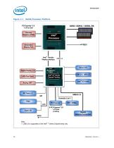
Mobile Processor Platform Intel® Processor PECI Embedded Display Port Intel® Flexible Display Interface Intel® Management Engine Intel® 6/7 Series Chipset Families LVDS Flat Panel WiFi / WiMax Gigabit Network Connection Note: 1. USB 3.0 is supported on the Intel® 7 Series Chipset family only.
Open the catalog to page 12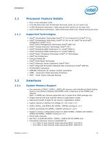
Processor Feature Details • • • • Four or two execution cores A 32-KB instruction and 32-KB data first-level cache (L1) for each core A 256-KB shared instruction / data second-level cache (L2) for each core Up to 8-MB shared instruction / data third-level cache (L3), shared among all cores Supported Technologies • Intel® Virtualization Technology (Intel® VT) for Directed I/O (Intel® VT-d) • Intel® Virtualization Technology (Intel® VT) for IA-32, Intel® 64 and Intel® Architecture (Intel® VT-x) Intel® Active Management Technology (Intel® AMT) 8.0 • Intel® Trusted Execution Technology (Intel® TXT)...
Open the catalog to page 13
• Processor on-die Reference Voltage (VREF) generation for both DDR3 Read (RDVREF) and Write (VREFDQ) • 1Gb, 2Gb, and 4Gb DDR3 DRAM device technologies are supported — Using 4Gb DRAM device technologies, the largest memory capacity possible is 32 GB, assuming Dual Channel Mode with four x8 dual ranked DIMM memory configuration • Up to 64 simultaneous open pages, 32 per channel (assuming 8 ranks of 8 bank devices) • Command launch modes of 1N/2N • On-Die Termination (ODT) • Asynchronous ODT • Intel® Fast Memory Access (Intel® FMA): — Just-in-Time Command Scheduling — Command Overlap — Out-of-Order...
Open the catalog to page 14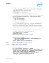
• PCI Express* extended configuration space. The first 256 bytes of configuration space aliases directly to the PCI Compatibility configuration space. The remaining portion of the fixed 4-KB block of memory-mapped space above that (starting at 100h) is known as extended configuration space. • PCI Express* Enhanced Access Mechanism. Accessing the device configuration space in a flat memory mapped fashion. • Automatic discovery, negotiation, and training of link out of reset • Traditional AGP style traffic (asynchronous non-snooped, PCI-X Relaxed ordering) • Peer segment destination posted write...
Open the catalog to page 15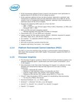
• 64-bit downstream address format; however, the processor never generates an address above 64 GB (Bits 63:36 will always be zeros) • 64-bit upstream address format, but the processor responds to upstream read transactions to addresses above 64 GB (addresses where any of Bits 63:36 are nonzero) with an Unsupported Request response. Upstream write transactions to addresses above 64 GB will be dropped. • Supports the following traffic types to or from the PCH: — DMI -> DRAM — DMI -> processor core (Virtual Legacy Wires (VLWs), Resetwarn, or MSIs only) — Processor core -> DMI • APIC and MSI interrupt...
Open the catalog to page 16
Embedded DisplayPort* (eDP*) • Stand alone dedicated port (unlike two generations ago that shared pins with PCIe interface) Intel® Flexible Display Interface (Intel® FDI) • For SKUs with graphics, carries display traffic from the Processor Graphics in the processor to the legacy display connectors in the PCH • Based on DisplayPort standard • The two Intel FDI links are capable of being configured to support three independent channels, one for each display pipeline • There are two Intel FDI channels, each one consists of four unidirectional downstream differential transmitter pairs: — Scalable...
Open the catalog to page 17
Processor Graphics Controller (GT) • • • • Intel® Rapid Memory Power Management (Intel® RMPM) – CxSR Intel® Graphics Performance Modulation Technology (Intel® GPMT) Intel® Smart 2D Display Technology (Intel® S2DDT) Graphics Render C-State (RC6) • Intel Seamless Display Refresh Rate Switching with eDP port Thermal Management Support • Digital Thermal Sensor • Intel Adaptive Thermal Monitor • THERMTRIP# and PROCHOT# support • On-Demand Mode • Open and Closed Loop Throttling • Memory Thermal Throttling • External Thermal Sensor (TS-on-DIMM and TS-on-Board) • Render Thermal Throttling • Fan speed...
Open the catalog to page 18All Intel catalogs and technical brochures
 10th Gen Intel® Core
7 Pages
 10th Gen
8 Pages
 nuc-celeron
4 Pages
 Intel® NUC 8 Home Mini PC
4 Pages
 Intel® Xeon® Scalable Platform
14 Pages
 Intel® Ethernet Controller XL710
1726 Pages
 Intel® Xeon® Processor E3-1200 v5
130 Pages
 Intel® Quark™ SoC X1000 Series
934 Pages
 Intel® X99 Chipset
4 Pages
 Intel® Desktop Board DQ67EP
4 Pages
 Intel® Ethernet Switch FM4000
270 Pages
 Intel® NUC Board DE3815TYBE
82 Pages
 S2600GZ and S2600GL
245 Pages
 i7-lga2011
314 Pages
 c600-series
936 Pages
 b75-express
4 Pages
 desktop-board
4 Pages
 3rd-gen-core-desktops
2 Pages
 /3rd-gen-core
2 Pages


Archived catalogs
 Intel® Ethernet Controllers
2 Pages
 Intel® 3450 Chipset
2 Pages
 Intel® 3000 and 3010 Chipset
4 Pages
 Intel® X58 Express Chipset
4 Pages
 Intel® Server Board S1200BT
8 Pages
 Intel® Desktop Board DX58SO2
4 Pages


- Management software solution
- Analysis software solution
- Real-time software
- Computer-aided design software
- Cloud-based software
- Design software solution
- Monitoring software solution
- Interface software
- Visualization software solution
- Simulation software solution
- Programming software
- Development software
- Network software
- Creation software
- Test software
- Wireless module
- Optimization software
- Solid-state drive
- Internal solid-state drive
- High-performance software