

Intel® Core? i7 Processor for LGA2011 Socket: Datasheet, Vol. 2

Intel® Core? i7 Processor for LGA2011 Socket: Datasheet, Vol. 2
This document is the second volume of the datasheet for the Intel® Core™ i7 Processor Family designed for the LGA2011 socket. It supports the Intel® Core™ i7-4960X Extreme Edition and other i7-49xx and i7-48xx series processors. The document includes legal disclaimers, emphasizing that Intel provides no warranty for the use of its products in mission-critical applications and that specifications may change without notice.
This section details the platform configuration structure, including processor IIO and uncore devices. It explains configuration register rules, such as CSR access, PCI bus numbers, and device mapping. Memory-mapped I/O registers and register terminology are also covered.
The document provides an extensive list of configuration registers for the Integrated Memory Controller. It includes detailed descriptions of various registers such as pxpcap, mcmtr, and tadwayness, among others. Each register's function and configuration are explained, providing essential information for system designers.
- Intel's legal disclaimers highlight the absence of warranties for specific uses and potential changes in specifications.
- The document emphasizes the importance of consulting Intel's resources for the latest specifications and errata.
- Overclocking and virtualization technologies are discussed, with warnings about potential impacts on system stability and performance.
This datasheet is a technical resource for developers and engineers working with Intel's LGA2011 socket processors. It provides detailed information on configuration registers and system requirements, essential for optimizing processor performance and ensuring compatibility.
The document includes a glossary of terms such as DDR3, DMA, DMI2, and Intel® Turbo Boost Technology, among others. These terms are essential for understanding the processor's functionalities and features.
A list of related documents is provided for further reference, including datasheets, thermal mechanical specifications, and design guides.
The processor IIO includes devices such as the DMI2 Root Port, PCI Express* Root Ports, and the Integrated I/O Core. Each device contains specific registers for configuration and management.
These devices are mapped on the PCI bus assigned to the processor socket and include the Processor Power Control Unit, Processor Interrupt Event Handling, Processor Core Broadcast, Processor Home Agent, and Integrated Memory Controllers. Each device has specific functions and registers for configuration and performance monitoring.
This section outlines the mapping of various processor uncore devices, including the Integrated Memory Controller, Processor Core Broadcast, CPU Interrupt Handling, CPU Home Agents, Performance Monitoring, Power Control Unit, and DDRIO. Each device is associated with specific bus numbers and functions, which are crucial for configuration and performance monitoring.
The processor supports different types of configuration registers, including PCI Configuration Registers, Machine Specific Registers, and Memory-Mapped I/O Registers. The document explains how these registers are accessed and the rules governing their use, such as the use of little-endian ordering for multi-byte numeric fields.
Each processor component is identified by a PCI bus address, consisting of Bus Number, Device Number, and Function Number. The document explains how bus numbers are derived and the significance of the CPUBUSNO register in determining the bus number for PCIe devices.
The document discusses the handling of unimplemented devices and functions, noting that configuration reads to these will return all ones, emulating a master abort response. It also describes the mechanism for hiding devices from host configuration software using the DEVHIDE register.
This section explains the role of memory-mapped I/O registers in driver programming and how they are accessed through processor reads and writes. It highlights the integration of chipset functionality that includes these registers.
The document provides a comprehensive list of register attributes, such as Read Only, Read/Write, and Write 1 to Set, among others. It explains the significance of each attribute and how they affect register behavior.
The document outlines the conventions used for representing hexadecimal, binary, and decimal numbers, ensuring clarity in the documentation of register addresses and values.
This section provides a detailed address map for the IMC Device 15 Function 0, listing various registers, their offsets, sizes, and descriptions. It includes information on PCI Express Capability and other configuration details.
- Bits 7 and 3 must be programmed to zero as upper and lower channel slot #3 are not supported.
- Bits 6-4 and 2-0 indicate the presence of TSOD sensors in various slots of upper and lower channels.
- SMB_TSOD_POLL_RATE_CNTR: This counter resets or loads a new value when decremented to zero, affecting the TSOD poll rate.
- SMBus Clock Period Configuration: Includes settings for clock period and time-out configurations, with specific values for different time-out durations.
- Configuration registers for DIMM memory technology include settings for rank disable control, DIMM population, rank count, DDR3 width, and density.
- Specific bits control the disabling of ranks and the configuration of DDR3 width and density.
- chn_temp_cfg: Controls temperature tracking and thermal bandwidth throttling.
- dimm_temp_oem: Sets threshold values for system interrupts based on temperature changes.
- dimm_temp_th: Configures thresholds for critical, high, and mid-level temperature alerts.
- dimm_temp_ev_ofst: Manages temperature averaging and MEMHOT event assertions based on temperature thresholds.
- Registers for device functions and capabilities, including PCI Express compliance and capability pointers.
- Specific offsets and default values are provided for each configuration setting.
1. Events are asserted when temperature thresholds (TEMPHI, TEMPMID, TEMPLO, TEMPOEMLO, TEMPOEMHI) are crossed. Each event triggers a configurable interrupt, either MEMHOT# or both SMI and MEMHOT#, as defined in bit 30 of CHN_TEMP_CFG.
- The DIMM temperature is used for thermal throttling and can be manipulated for testing when unlocked. The temperature range is 0 to 127°C, with a default of 85°C to prevent refresh issues during certain operations.
- Power throttling is controlled by the THRT_PWR_EN bit, allowing a maximum number of transactions during a 1 µs timeframe. This can be dynamically updated by PCODE.
- Various timing parameters are defined for DDR3 operations, including T_RAS, T_CWL, T_CL, T_RP, T_RCD, and others. These parameters ensure proper operation and prevent timing violations.
- Refresh timing parameters like T_RFC and T_REFI are specified for different DDR3 speeds. ZQ calibration timing is also defined to ensure proper operation.
- MR2 and MR0 shadow registers are used for storing configuration settings related to address swizzling and mode register settings.
- Set panic and high watermark levels for refresh priorities to optimize refresh periods. Ensure timing parameters meet DDRIO requirements to avoid violations.
- DDDC can be enabled on supported systems through BIOS settings, allowing for faster sparing with SDDC substitution.
- The Fail Device ID captures the ID of a failed device upon successful correction, with a valid range of 0-35 for x4 devices.
- Details on various registers and their offsets are provided, including device IDs, command statuses, and configuration registers.
- The UBOX handles non-mainstream flows such as register accesses and interrupt flows.
- Registers include CPUNODEID, IntControl, GIDNIDMAP, CoreCount, and UBOXErrSts, each with specific configurations and functions.
- Registers report thermal status, accumulated bandwidth, and power settings for memory channels.
- PACKAGE_POWER_SKU defines power and timing parameters, while PACKAGE_ENERGY_STATUS tracks energy consumption.
- Temperature and power units are defined for various registers, impacting how power and thermal data are calculated and reported.
- P-State limits allow software to control maximum frequency during runtime.
- Secondary Status Register: Contains bits for detecting parity errors, system errors, and master abort statuses.
- Primary Bus Number Register: Used to program the bus number on the primary side of the bridge.
- Memory Base and Limit Registers: Define memory address ranges for PCI Express* ports, ensuring proper forwarding of memory transactions.
- Prefetchable Memory Base and Limit Registers: Manage 64-bit prefetchable memory address ranges for efficient data handling.
The memory address range is aligned to a 1MB boundary, with the top of the range being one less than a 1MB boundary. The bottom 4 bits of the Prefetchable Memory Base and Limit registers indicate if the bridge supports 64-bit addresses. A value of 0h means only 32-bit addresses are supported, while 1h indicates 64-bit support, utilizing additional registers for the upper 32 bits. Setting the memory limit below the base disables the 64-bit range.
- Capability Pointer (capptr): Points to the first capability structure, specifically the PCIe capability.
- Interrupt Line and Pin Registers (intl, intpin): These registers are not applicable for the devices mentioned.
- Bridge Control Register (bctrl): Controls various functions such as hot reset, VGA I/O decoding, and error message forwarding.
- Subsystem Capability Identity (scapid): Assigned by PCI-SIG for subsystem capability ID.
- MSI Capability (msicapid, msinxtptr, msimsgctl): Details the MSI capability ID, next pointer, and control settings for MSI interrupts.
- PCI Express Capability (pxpcapid, pxpnxtptr, pxpcap): Provides PCI Express capability ID and related settings.
- Device Capabilities (devcap): Identifies device-specific information, including slot implementation and device port type.
- Device Control (devctrl): Manages device control settings, such as extended tag field support and maximum payload size.
- Configuration Registers: The document details several configuration registers, including root control, root capabilities, and root status. Each register is associated with specific bus, device, and function numbers, and has a unique offset.
- Bit Descriptions: Each register contains multiple bits with specific attributes (e.g., Read-Write, Read-Only) and default values. The document explains the purpose of each bit, such as enabling error notifications, controlling interrupt generation, and managing completion timeouts.
- Error Handling: The document describes how the system handles different types of errors (fatal, non-fatal, and correctable) and the role of internal IIO core error logic in escalating these errors.
- Link Capabilities and Control: It outlines the supported link speeds and the mechanisms for controlling link compliance and speed adjustments. Specific bits are used to manage de-emphasis levels and compliance testing.
- Power Management Events (PME): The document explains how PME messages are handled, including the indication of pending PMEs and the process for clearing PME status bits.
- Error Notification: System error notifications can be generated for fatal, non-fatal, and correctable errors, with options for both system errors and MSI/INTx interrupts.
- Completion Timeout: The document provides detailed encoding for completion timeout values, allowing system software to modify timeout ranges for transactions.
- Link Speed Management: The document specifies how link speeds are supported and managed, including the impact of hardware settings like the Gen3OFF fuse.
- Uncorrectable Error Severity (uncerrsev): Indicates the severity of uncorrectable errors.
- Correctable Error Status (corerrsts): Identifies the status of correctable errors detected by the PCI Express port.
- Correctable Error Mask (corerrmsk): Masks correctable errors from being signaled.
- Advanced Error Capabilities and Control Register (errcap): Manages advanced error capabilities.
- Root Port Error Command (rperrcmd): Controls behavior upon detection of errors.
- Root Port Error Status (rperrsts): Reports the status of error messages received by the Root Complex and errors detected by the Root Port.
- Error Source Identification (errsid): Logs the Requestor ID of the source when an error message is received.
- Performance Control and Status Register 0 (perfctrlsts_0): Manages performance-related settings such as outstanding requests and flow control.
- Performance Control and Status Register 1 (perfctrlsts_1): Further controls performance parameters.
- MISC Control and Status Register 0 (miscctrlsts_0): Includes settings for TLP Processing Hint, DCA Requester ID Override, and other miscellaneous controls.
- MISC Control and Status Register 1 (miscctrlsts_1): Manages system error settings and other miscellaneous controls.
- Registers are categorized by type, port ID, bus, device, function, and offset.
- Each register has specific bits with attributes such as Read/Write (RW), Read-Only (RO), and Read-Write-Set (RWS).
- Default values are provided for each bit, indicating the initial state of the register.
- Recommendations for BIOS settings are included, particularly for performance optimization and error handling.
- The VC Enable bit indicates whether a Virtual Channel is enabled or disabled. A '1' indicates enabled, and a '0' indicates disabled. The VC Negotiation Pending bit must be cleared to confirm VC enablement.
- BIOS requirements for VC management include setting VC Enable bits in both components on a link to enable a VC, ensuring no traffic uses a VC when disabling it, and fully disabling a VC before re-enabling it.
- Traffic Class 7 is always routed to VCm, while Traffic Class 0 is always routed to VC0. The mapping of other Traffic Classes to VC resources is indicated by specific bits.
- The DMI VCP Resource Status and DMI VCM Resource Capability sections report the status and capabilities of VC resources, including negotiation status and credit throttling.
- The VC Negotiation Pending bit indicates whether the VC negotiation process is complete.
- Credit throttling controls the number of credits withheld for posted and non-posted requests for VC1, VCp, and VCm.
- The document details various configuration registers for Integrated I/O (IIO) devices, including vendor and device identification numbers, command and status registers, and capability pointers.
- Specific registers control aspects like cacheline size, multifunction device status, and PCI Express capabilities.
- Software must ensure VC negotiation is complete before using a VC and must manage traffic class mappings and credit throttling appropriately.
- BIOS must adhere to specific requirements for enabling and disabling VCs, ensuring no traffic is present during these operations.
- Maximum Handle Mask Value: IIO supports all 16 bits of handle being masked. However, the hardware does not consider the mask value during global interrupt entry invalidation.
- Invalidation Unit Offset: Invalidation registers are located at offset 200h.
- Snoop Control: Hardware supports the 1-setting of the SNP field in page-table entries for non-isoch Intel VT-d engine.
- Pass Through: Supported by IIO, with defeaturing option for post-silicon bugs.
- IA32 Extended Interrupt Mode: Supported by IIO.
- Interrupt Remapping Support: Supported by IIO.
- Device TLB Support: Supported for non-isoch Intel VT-d engine, with defeaturing option for post-silicon bugs.
- Queued Invalidation Support: Supported by IIO.
- Coherency Support: BIOS can write to indicate snoop or non-snoop for DMA/Interrupt table structures, expected to be set to 0 for Intel VT-d engine.
- Translation Enable: Software must set up DMA-remapping structures, flush write buffers, set root-entry table pointer, perform global invalidation of context-cache and IOTLB, and set up fault log pointer if advanced fault logging is supported before enabling DMA-remapping hardware.
- Set Root Table Pointer: Must be performed before enabling DMA remapping hardware. Requires global invalidation of context cache and IOTLB.
- Queued Invalidation Enable: Software must ensure all prior invalidations are completed before enabling queued invalidations.
- Interrupt Remapping Enable: Requires setup of interrupt-remapping structures and global invalidation of IOTLB.
- Ensure deterministic transaction boundaries when enabling/disabling remapping logic to handle in-flight transactions appropriately.
- Update root table and interrupt remap table pointers only when necessary and ensure new structures provide the same remapping results as previous ones.
- Fault Record Index: Indicates the index of the fault recording register for the first pending fault.
- Invalidation Timeout Error: Detected when Device-IOTLB invalidation completion times out.
- Invalidation Completion Error: Occurs when an unexpected or invalid Device-IOTLB invalidation completion is received.
- Invalidation Queue Error: Detected when there is an error associated with the invalidation queue.
Catalog excerpts

Intel® Core™ i7 Processor Family for LGA2011 Socket Datasheet – Volume 2 of 2 Supporting Desktop Intel® Core™ i7-4960X Extreme Edition Processor Series for the LGA2011 Socket Supporting Desktop Intel® Core™ i7-49xx and i7-48xx Processor Series for the LGA2011 Socket
Open the catalog to page 1
INFORMATION IN THIS DOCUMENT IS PROVIDED IN CONNECTION WITH INTEL PRODUCTS. NO LICENSE, EXPRESS OR IMPLIED, BY ESTOPPEL OR OTHERWISE, TO ANY INTELLECTUAL PROPERTY RIGHTS IS GRANTED BY THIS DOCUMENT. EXCEPT AS PROVIDED IN INTEL'S TERMS AND CONDITIONS OF SALE FOR SUCH PRODUCTS, INTEL ASSUMES NO LIABILITY WHATSOEVER AND INTEL DISCLAIMS ANY EXPRESS OR IMPLIED WARRANTY, RELATING TO SALE AND/OR USE OF INTEL PRODUCTS INCLUDING LIABILITY OR WARRANTIES RELATING TO FITNESS FOR A PARTICULAR PURPOSE, MERCHANTABILITY, OR INFRINGEMENT OF ANY PATENT, COPYRIGHT OR OTHER INTELLECTUAL PROPERTY RIGHT. Legal Lines...
Open the catalog to page 2
Revision History Revision Number 001 Initial release
Open the catalog to page 13
(This page intentionally left blank)
Open the catalog to page 14
Introduction This document is Volume 2 of 2 of the datasheet for the Intel® Core™ i7 processor family for LGA2011 Socket. Volume 2 provides register information for these processors. Volume 2 of 2 describes the Configuration Status Registers (CSRs) of each individual functional block in Uncore logic. The processor contains one or more PCI devices within each individual functional block. CSRs are the basic hardware elements that configure the Uncore logic to support various system topologies, memory configuration, and densities. The processor family contains one or more PCI devices within a single...
Open the catalog to page 15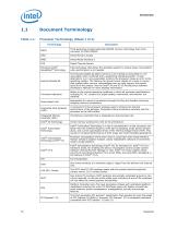
Document Terminology Processor Terminology (Sheet 1 of 2) Terminology Third generation Double Data Rate SDRAM memory technology that is the successor to DDR2 SDRAM Direct Memory Access Direct Media Interface 2 Digital Thermal Sensor Enhanced Intel® SpeedStep® Technology Intel technology that allows the operating system to reduce power consumption when performance is not needed. The Execute Disable bit allows memory to be marked as executable or nonexecutable–when combined with a supporting operating system. If code attempts to run in non-executable memory the processor raises an error to the...
Open the catalog to page 16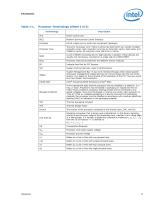
Processor Terminology (Sheet 2 of 2) Terminology Power Control Unit Platform Environment Control Interface 64-bit, single-core or multi-core component (package) Processor Core The term “processor core” refers to silicon die itself which can contain multiple execution cores. Each execution core has an instruction cache, data cache, and 256KB L2 cache. All execution cores share the L3 cache. A unit of DRAM connecting four to eight devices in parallel. These devices are usually, but not always, mounted on a single side of a DDR3 DIMM. Processor interconnect between the different Uncore modules Indicate...
Open the catalog to page 17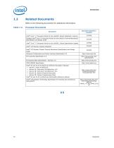
Related Documents Refer to the following documents for additional information. Processor Documents Document Document Number/ Location Intel® Core™ i7 Processor Family for the LGA2011 Socket Datasheet, Volume 1 Desktop Intel Core™ i7 Processor Family for the LGA2011 Thermal Mechanical Specification and Design Guide Intel® Core™ i7 Processor Family for the LGA2011 Socket Specification Update Intel® X79 Express Chipset Datasheet Intel® X79 Express Chipset Thermal Mechanical Specifications and Design Guide Advanced Configuration and Power Interface Specification 3.0 http://www.pcisig.com/ specifications...
Open the catalog to page 18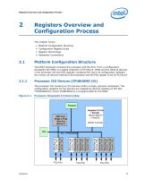
Registers Overview and Configuration Process Registers Overview and Configuration Process This chapter covers • • • • Platform Configuration Structure Configuration Register Rules Register Terminology Notational Conventions Platform Configuration Structure The DMI2 physically connects the processor and the PCH. From a configuration standpoint the DMI2 is a logical extension of PCI Bus 0. DMI2 and the internal devices in the processor IIO and PCH logically constitute PCI Bus 0 to configuration software. As a result, all devices internal to the processor and the PCH appear to be on PCI Bus 0. Processor...
Open the catalog to page 19
Registers Overview and Configuration Process • Device 0: DMI2 Root Port. Logically this appears as a PCI device residing on PCI Bus 0. Device 0 contains the standard PCI header registers, extended PCI configuration registers and DMI2 device specific configuration registers. • Device 1: PCI Express* Root Port 1a, 1b. Logically this appears as a “virtual” PCI-to-PCI bridge residing on PCI Bus 0 and is compliant with PCI Express* Local Bus Specification Revision 2.0. Device 1 contains the standard PCI Express*/PCI configuration registers including PCI Express* Memory Address Mapping registers. It...
Open the catalog to page 20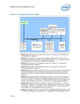
Registers Overview and Configuration Process Processor Uncore Devices Map Bus = CPUBUSNO (1)* Power Control Unit (PCU) (Device 10, Function 0‐ 4) Integrated Memory Controller (Device 15 General Registers, TAD Rank and Timings, Device 16 Thermal Control and Test Registers) Performance Monitoring (Device 14,16,19) • Device 10: Processor Power Control Unit. Device 10, Function 0-4 contains the configurable PCU registers. • Device 11: Processor Interrupt Event Handling (UBox). Device 11, Function 0 contains the processor Interrupt Control Registers. Device 11, Function 3 contains the Semaphore...
Open the catalog to page 21
Registers Overview and Configuration Process • Device 19: Processor Performance Monitoring and Ring. Device 19 Function 0 contains the processor ring to PCI Express agent. Device 19, Function 1 contains the processor Ring to PCI Express performance monitoring registers. Device 19, Function 4 -6 contains the processor performance monitoring registers. • Device 22: Processor Core Broadcast. Device 22 Function 1-2 contains the Caching agent broadcast configuration registers for the Memory Controller. Device 22 Function 0 contains the System Address Decode Registers. Configuration Register Rules...
Open the catalog to page 22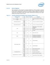
Registers Overview and Configuration Process Device Mapping Each component in the processor is uniquely identified by a PCI bus address consisting of Bus Number, Device Number, and Function Number. Device configuration is based on the PCI Type 0 configuration conventions. All processor registers appear on the PCI bus assigned for the processor socket. Bus number is derived by the maximum bus range setting and processor socket number. Functions Specifically Handled by the Processor (Sheet 1 of 2) Register Group x4 Link from Processor to PCH Device 0 will work as a x4 PCI Express Port PCI Express...
Open the catalog to page 23All Intel catalogs and technical brochures
 10th Gen Intel® Core
7 Pages
 10th Gen
8 Pages
 nuc-celeron
4 Pages
 Intel® NUC 8 Home Mini PC
4 Pages
 Intel® Xeon® Scalable Platform
14 Pages
 Intel® Ethernet Controller XL710
1726 Pages
 Intel® Xeon® Processor E3-1200 v5
130 Pages
 Intel® Quark™ SoC X1000 Series
934 Pages
 Intel® X99 Chipset
4 Pages
 Intel® Desktop Board DQ67EP
4 Pages
 Intel® Ethernet Switch FM4000
270 Pages
 Intel® NUC Board DE3815TYBE
82 Pages
 S2600GZ and S2600GL
245 Pages
 i7-lga2011
314 Pages
 c600-series
936 Pages
 b75-express
4 Pages
 desktop-board
4 Pages
 3rd-gen-core-desktops
2 Pages
 /3rd-gen-core
2 Pages


Archived catalogs
 Intel® Ethernet Controllers
2 Pages
 Intel® 3450 Chipset
2 Pages
 Intel® 3000 and 3010 Chipset
4 Pages
 Intel® X58 Express Chipset
4 Pages
 Intel® Server Board S1200BT
8 Pages
 Intel® Desktop Board DX58SO2
4 Pages


- Management software solution
- Analysis software solution
- Real-time software
- Computer-aided design software
- Cloud-based software
- Design software solution
- Monitoring software solution
- Interface software
- Visualization software solution
- Simulation software solution
- Programming software
- Development software
- Network software
- Creation software
- Test software
- Wireless module
- Optimization software
- Solid-state drive
- Internal solid-state drive
- High-performance software