Intel® Core? i7-600/i5-500/i5-400/i3-300 Processor Series: Vol. 2
1 /388Pages

Intel® Core? i7-600/i5-500/i5-400/i3-300 Processor Series: Vol. 2
1 /388Pages
Catalog excerpts
Intel® Core™ i7-600, i5-500, i5-400 and i3-300 Mobile Processor Series Datasheet — Volume Two This is volume 2 of 2. Refer to Document Number 322812 for Volume 1 November 2010
Open the catalog to page 1
INFORMATION IN THIS DOCUMENT IS PROVIDED IN CONNECTION WITH INTEL® PRODUCTS. NO LICENSE, EXPRESS OR IMPLIED, BY ESTOPPEL OR OTHERWISE, TO ANY INTELLECTUAL PROPERTY RIGHTS IS GRANTED BY THIS DOCUMENT. EXCEPT AS PROVIDED IN INTEL'S TERMS AND CONDITIONS OF SALE FOR SUCH PRODUCTS, INTEL ASSUMES NO LIABILITY WHATSOEVER, AND INTL DISCLAIMS ANY EXPRESS OR IMPLIED WARRANTY, RELATING TO SALE AND/OR USE OF INTEL PRODUCTS INCLUDING LIABILITY OR WARRANTIES RELATING TO FITNESS FOR A PARTICULAR PURPOSE, MERCHANTABILITY, OR INFRINGEMENT OF ANY PATENT, COPYRIGHT OR OTHER INTELLECTUAL PROPERTY RIGHT. Intel products...
Open the catalog to page 2
Figures Figure Figure Figure Figure Figure Figure Figure Figure Figure Figure Tables Table Table Table Table
Open the catalog to page 10
Revision History Revision Number Revision Date • Initial Release • Updated Figure 8 for better clarification
Open the catalog to page 11
Processor Configuration Registers Processor Configuration Registers This is volume 2 of the Intel Core i7-600, i5-500, i5-400 and i3-300 Mobile Processor Series Datasheet. Throughout this document, the Intel Core i7-600, i5-500, i5-400 and i3-300 Mobile Processor Series may be referred to as simply the processor. This document provides register information for the processor. Register Terminology The following table shows the register-related terminology that is used in this document. (Sheet 1 of 3) Item Read Only bit(s). Writes to these bits have no effect. These are static values only. Read...
Open the catalog to page 12
Processor Configuration Registers Read/Write 1 to Clear/Lockable/Sticky bit(s). These bits can be read. Internal events may set this bit. A software write of 1 clears (sets to 0) the corresponding bit(s) and a write of 0 has no effect. Bits are not cleared by “warm” reset, but is reset with a cold/complete reset (for PCI Express related bits a cold reset is “Power Good Reset” as defined in the PCI Express Base spec). Additionally there is a Key bit (which is marked RW-K or RW-L-K) that, when set, prohibits this bit field from being writable (bit field becomes Read Only/Volatile). Read/Write 1...
Open the catalog to page 13
Processor Configuration Registers Write-only. These bits may be written by software, but will always return zeros when read. They are used for write side-effects. Any data written to these registers cannot be retrieved. Read/Write Once/Sticky bit(s). Reads prior to the first write return the default value. The first write after cold reset stores any value written. Any subsequent write to this bit field is ignored. All subsequent reads return the first value written. The value returns to default on cold reset. If there are multiple RW-O or RW-O-S fields within a DWORD, they should be written all...
Open the catalog to page 14
Processor Configuration Registers When running in internal graphics mode, tileX/tileY/linear reads/writes to GMADR range are supported. Write accesses to GMADR linear regions are supported from both DMI and PEG. GMADR write accesses to tileX and tileY regions (defined via fence registers) are not supported from DMI or the PEG port. GMADR read accesses are not supported from either DMI or PEG. In the following sections, it is assumed that all of the compatibility memory ranges reside on the DMI Interface. The exception to this rule is VGA ranges, which may be mapped to PCI Express*, DMI, or to...
Open the catalog to page 15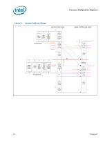
HOST/SYSTEM VIEV (DRAM CONTROLLER VIEV
Open the catalog to page 16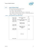
Processor Configuration Registers Legacy Address Range This area is divided into the following address regions: • 0 – 640 KB – Microsoft MS-DOS* Area • 640 – 768 KB – Legacy Video Buffer Area • 768 – 896 KB in 16 KB sections (total of 8 sections) – Expansion Area • 896 – 960 KB in 16 KB sections (total of 4 sections) – Extended System BIOS Area • 960 KB – 1-MB Memory – System BIOS Area Figure 2. Microsoft MS-DOS* Legacy Address Range System BIOS (Upper) 64KB Extended System BIOS (Lower) 64KB (16KBx4) 000B_FFFFh Legacy Video Area (SMM Memory) 128KB 000A_0000h
Open the catalog to page 17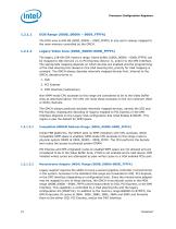
Processor Configuration Registers DOS Range (0000_0000h – 0009_FFFFh) The DOS area is 640 KB (0000_0000h – 0009_FFFFh) in size and is always mapped to the main memory controlled by the GMCH. Legacy Video Area (000A_0000h-000B_FFFFh) The legacy 128-KB VGA memory range, frame buffer, (000A_0000h – 000B_FFFFh) can be mapped to IGD (Device 2), to PCI Express (Device 1), and/or to the DMI Interface. The appropriate mapping depends on which devices are enabled and the programming of the VGA steering bits. Based on the VGA steering bits, priority for VGA mapping is constant. The GMCH always decodes...
Open the catalog to page 18
Processor Configuration Registers PAM (000C_0000h-000F_FFFFh) The 13 sections from 768 KB to 1 MB comprise what is also known as the PAM Memory Area. Each section has Read enable and Write enable attributes. The CPU documentation will now contain the registers and decode rules/restrictions. The PAM registers have moved to the CPU. For the PAM register details, refer to CPU documentation. • ISA Expansion Area (000C_0000h-000D_FFFFh) • Extended System BIOS Area (000E_0000h-000E_FFFFh) • System BIOS Area (000F_0000h-000F_FFFFh) The CPU contains the PAM registers and the GMCH has no knowledge of...
Open the catalog to page 19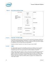
Processor Configuration Registers Main Memory Address Range FFFF_FFFFh FLASH APIC LT Contains: Dev 0, 1, 2, 6, 7 BARS & ICH/PCI ranges PCI Memory Range TOLUD IGD IGGTT TSEG TSEG_BASE DPR Main Memory ISA Hole (15 MB-16 MB) This register moved to the CPU. As such, the CPU performs the necessary decode and routes the request appropriately. Specifically, if no hole is created, the CPU will route the request to DRAM (HOM channel). If a hole is created, the CPU will route the request on NCS/NCB, since the request does not target DRAM. Graphics translated requests to the range will always route to DRAM....
Open the catalog to page 20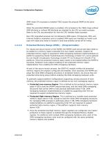
Processor Configuration Registers SMM-mode CPU accesses to enabled TSEG access the physical DRAM at the same address. When the extended SMRAM space is enabled, CPU accesses to the TSEG range without SMM attribute or without WB attribute are handled by the CPU as invalid accesses. Refer to the CPU documentation for how the CPU handles these accesses. Non-CPU originated accesses are not allowed to SMM space. PCI-Express, DMI, and Internal Graphics originated cycle to enabled SMM space are handled as invalid cycle type with reads and writes to location 0 and byte enables turned off for writes. Protected...
Open the catalog to page 21All Intel catalogs and technical brochures
 10th Gen Intel® Core
7 Pages
 10th Gen
8 Pages
 nuc-celeron
4 Pages
 Intel® NUC 8 Home Mini PC
4 Pages
 Intel® Xeon® Scalable Platform
14 Pages
 Intel® Ethernet Controller XL710
1726 Pages
 Intel® Xeon® Processor E3-1200 v5
130 Pages
 Intel® Quark™ SoC X1000 Series
934 Pages
 Intel® X99 Chipset
4 Pages
 Intel® Desktop Board DQ67EP
4 Pages
 Intel® Ethernet Switch FM4000
270 Pages
 Intel® NUC Board DE3815TYBE
82 Pages
 S2600GZ and S2600GL
245 Pages
 i7-lga2011
314 Pages
 c600-series
936 Pages
 b75-express
4 Pages
 desktop-board
4 Pages
 3rd-gen-core-desktops
2 Pages
 /3rd-gen-core
2 Pages


Archived catalogs
 Intel® Ethernet Controllers
2 Pages
 Intel® 3450 Chipset
2 Pages
 Intel® 3000 and 3010 Chipset
4 Pages
 Intel® X58 Express Chipset
4 Pages
 Intel® Server Board S1200BT
8 Pages
 Intel® Desktop Board DX58SO2
4 Pages


- Bourn And Koch management software
- Bourn And Koch analysis software
- Bourn And Koch real-time software
- Bourn And Koch CAD software
- Bourn And Koch cloud software
- Bourn And Koch design software
- Bourn And Koch monitoring software
- Bourn And Koch interface software
- Visualization software solution
- Bourn And Koch simulation software
- Bourn And Koch programming software
- Development software
- Bourn And Koch network software
- Creation software
- Bourn And Koch optimization software
- Bourn And Koch test software
- Wireless module
- Bourn And Koch solid-state drive
- Bourn And Koch internal solid-state drive
- High-performance software