
2nd Generation Intel® Core? Mobile Processor Datasheet, Vol. 1

2nd Generation Intel® Core? Mobile Processor Datasheet, Vol. 1
This document is the first volume of a datasheet for the 2nd Generation Intel® Core™ Processor Family Mobile and Intel® Celeron® Processor Family Mobile. It provides detailed information on supported processor series, including Intel® Core™ i7 Mobile Extreme Edition, Intel® Core™ i5, i7 Mobile Processor Series, and Intel® Celeron® Mobile Processor Series.
The datasheet outlines various supported technologies such as Intel® Virtualization Technology, Intel® Trusted Execution Technology, and Intel® Turbo Boost Technology. It also covers system memory support, PCI Express interfaces, Direct Media Interface (DMI), and processor graphics capabilities.
The document details the system memory interface, including supported technologies, timing support, and organization modes. It also describes the PCI Express architecture, configuration mechanisms, and graphics support. The Direct Media Interface (DMI) and Platform Environment Control Interface (PECI) are also covered.
Key technologies discussed include Intel® Virtualization Technology, Intel® Trusted Execution Technology, Intel® Hyper-Threading Technology, and Intel® Advanced Vector Extensions. The document also highlights Intel® Advanced Encryption Standard New Instructions and Intel® 64 Architecture x2APIC.
The datasheet provides information on power management features, including Advanced Configuration and Power Interface (ACPI) states, processor core/package idle states, and integrated memory controller states. It also discusses PCI Express link states and Direct Media Interface (DMI) states.
The document includes legal disclaimers regarding the use of Intel products, emphasizing that the information is provided in connection with Intel products and that no license to any intellectual property rights is granted. It also notes that Intel products are not designed for applications where failure could result in personal injury or death.
- Enhanced Intel® SpeedStep® Technology: This technology allows the processor to adjust its voltage and core frequency to decrease power consumption and heat production.
- Low-Power Idle States: The processor can enter various low-power states (C-states) to conserve energy when idle. These include Core C0, C1/C1E, C3, C6, and C7 states, each progressively reducing power usage.
- Package C-States: Similar to core C-states, package C-states (C0, C1/C1E, C3, C6, C7) manage power at the package level, affecting the entire processor package.
- Disabling Unused System Memory Outputs: Unused memory outputs can be disabled to save power.
- DRAM Power Management: Includes features like Conditional Self-Refresh and Dynamic Power-down to manage DRAM power usage efficiently.
- Power management techniques are applied to PCI Express* and Direct Media Interface (DMI) to reduce power consumption during low activity periods.
- Intel® Rapid Memory Power Management (Intel® RMPM): Also known as CxSR, this feature helps manage memory power in graphics.
- Intel® Graphics Performance Modulation Technology (Intel® GPMT): Modulates graphics performance to save power.
- Display Power Savings Technology 6.0 (DPST): Reduces display power consumption by adjusting brightness and refresh rates.
- Thermal Design Power (TDP): The maximum amount of heat a cooling system is required to dissipate.
- Intel® Turbo Boost Technology: Allows processors to run above their base operating frequency to improve performance, with power and thermal management.
- Adaptive Thermal Monitor: Protects the processor from overheating by adjusting performance.
- Details various signal types including system memory interface signals, PCI Express*-based interface signals, and power sequencing signals.
- Includes power and ground pin specifications, voltage identification (VID), and decoupling guidelines to ensure stable processor operation.
- Provides detailed pin assignments and mechanical package information for different processor configurations.
The processor graphics feature a refreshed sixth-generation graphics core, offering improved performance and reduced power consumption with support for up to 12 Execution Units (EUs). It includes Intel Clear Video Technology HD for enhanced video playback and image quality, supporting HD content encoding/transcoding, Blu-ray Disc playback, and 3D content via HDMI. It also supports DirectX Video Acceleration for video processing and is compatible with multiple operating systems including Windows and Linux.
The eDP is a standalone dedicated port, while the Intel FDI carries display traffic from the processor graphics to legacy display connectors, based on the DisplayPort standard. It features two independent links and supports various display bandwidth requirements.
The processor supports various power management features including ACPI C-states, Enhanced Intel SpeedStep Technology, and Intel Rapid Memory Power Management. It also supports power management capabilities for PCI Express and Direct Media Interface.
Thermal management features include a digital thermal sensor, Intel Adaptive Thermal Monitor, and various throttling mechanisms to manage processor temperature and fan speed.
The processor is available in two package sizes: a 37.5 x 37.5 mm rPGA package and a 31 x 24 mm BGA package.
The Integrated Memory Controller supports DDR3 protocols with two 64-bit channels, supporting various DDR3 data transfer rates and SO-DIMM module configurations. It supports single-channel and dual-channel memory organization modes, with dual-channel symmetric mode providing maximum performance.
Intel Fast Memory Access technology includes enhancements like Just-in-Time Command Scheduling, allowing for efficient memory request handling and improved performance.
- Command Overlap: Allows insertion of DRAM commands between Activate, Precharge, and Read/Write commands to increase efficiency without affecting current commands.
- Out-of-Order Scheduling: Reorders requests to optimize bandwidth and reduce latency, especially for requests to the same open page.
- Memory Type Range Registers (MTRRs): Enhanced with two additional MTRRs to support larger system memory beyond 4 GB.
- Data Scrambling: Utilizes DDR3 Data Scrambling to minimize di/dt impact on the platform by creating pseudo-random patterns on the data bus.
- DRAM Clock Generation: Supported DIMMs have two differential clock pairs, with a total of four clock pairs driven by the processor.
- Architecture: Maintains compatibility with PCI addressing model, supporting Gen2 speed for increased bandwidth.
- Transaction Layer: Manages assembly and disassembly of Transaction Layer Packets (TLPs) and flow control.
- Data Link Layer: Handles link management, error detection, and correction, ensuring integrity of TLPs.
- Physical Layer: Includes circuitry for interface operation and converts data for transmission across the PCI Express Link.
- Configuration Mechanism: Extends configuration space to 4096 bytes per device/function, with enhanced access mechanisms.
- Error Flow: Generates SERR in response to errors, with no support for SCI, SMI, MSI, PCI INT, or GPE.
- Compatibility: Compatible with Intel® 6 Series Chipset PCH, not with previous PCH products.
- Link Down: A fatal error that hangs the system, preventing data corruption by not allowing link retraining.
- 3D and Video Engines: Includes 3D compute elements and multi-format decode/encode pipeline for improved performance.
- 3D Engine Execution Units: Supports up to 12 EUs with SIMD8 and SIMD16 instructions for vertex and pixel processing.
- Video Engine: Handles non-3D applications with support for VLD and MPEG2 decode in hardware.
- 2D Engine: Contains BLT functionality and supports extensive 2D instructions for GUI acceleration.
- Display Planes: Defines format and location of memory regions for display, supporting independent display streams with double-buffering.
- Sprite Planes: Optimized for video decode, associated with main display planes, and also double-buffered.
- Cursors A and B: Dedicated planes for mouse cursor acceleration, supporting resolutions up to 256 x 256.
- Video Graphics Array (VGA): Used for boot, safe mode, and legacy games, modifiable without OS/driver notification.
- Display Pipes: Blend and synchronize pixel data, operating independently at 1 pixel per clock, sending data via Intel Flexible Display Interface (Intel FDI).
- Display Ports: Transmit display data to devices like LVDS, HDMI, DVI, SDVO, with most interfaces driven from the PCH except DisplayPort.
- Embedded DisplayPort (eDP): Supports integrated display devices with link-speeds of 1.62 Gbps and 2.7 Gbps on multiple data lanes.
- Proprietary link for display traffic from Processor Graphics to PCH display I/Os, supporting two independent channels with dynamic scalability and a common 100-MHz reference clock.
- Supports simultaneous use of Processor Graphics Controller and a x16 PCI Express Graphics device, with a maximum of 2 displays connected to each.
- One-wire interface for communication between PECI client and master, allowing thermal information exchange and fan speed control.
- Internal clocking requirements with reference input clocks for various components.
- Intel® Virtualization Technology (Intel® VT): Enables multiple independent operating systems on a single system, with hardware support for improved performance and security.
- Intel® Trusted Execution Technology (Intel® TXT): Provides platform-level enhancements for creating trusted platforms, ensuring authenticity and resistance to unauthorized changes.
- Intel® Hyper-Threading Technology (Intel® HT): Allows an execution core to function as two logical processors, requiring BIOS and OS support.
- Intel® Turbo Boost Technology: Allows the processor to run faster than its rated frequency when conditions permit, enhancing performance for both multi-threaded and single-threaded workloads.
The Turbo Technology processor frequencies are activated when the operating system requests the P0 state. The graphics render frequency is dynamically selected based on workload demand, allowing for optimized performance through power sharing between processor cores and graphics cores. This technology requires the Intel Graphics driver to be properly installed.
Intel AVX extends the Intel SSE from 128-bit to 256-bit vectors, enhancing performance in scientific, engineering, and other applications. It offers improved performance through wider vectors and new functionalities.
Intel AES-NI provides a set of SIMD instructions for fast and secure data encryption and decryption based on AES. It includes six instructions that facilitate high-performance encryption and decryption, supporting a wide range of cryptographic applications.
The x2APIC architecture extends the xAPIC architecture to increase processor addressability and enhance interrupt delivery performance. It supports two modes of operation for backward compatibility and future extensibility, with increased processor addressability and efficient MSR interface access.
This section covers power management topics including ACPI states, processor core, integrated memory controller, PCI Express, and Direct Media Interface. The processor supports various ACPI states, with different power and performance characteristics.
This technology optimizes processor frequency and voltage based on workload, with multiple frequency and voltage points for optimal performance and power efficiency. It allows for software-controlled frequency selection and ensures glitch-free transitions.
Low-power idle states (C-states) are used to save power when the processor is idle. Higher C-states offer more power savings but have longer entry and exit latencies. The processor automatically resolves core C-states, and software interfaces like MWAIT and HLT are used to request low-power states.
- Core C0 State: Normal operating state where code execution occurs.
- Core C1/C1E State: Low power state entered via HLT or MWAIT(C1/C1E) instructions. Handles bus snoops and snoops from other threads.
- Core C3 State: Entered by P_LVL2 I/O read or MWAIT(C3). Caches are flushed to L3, and core clocks stop.
- Core C6 State: Entered by P_LVL3 I/O read or MWAIT(C6). Architectural state saved to SRAM, voltage reduced to zero.
- Core C7 State: Similar to C6, but last core entering C7 flushes L3 cache. Supports C7s substate for efficient L3 cache flushing.
- C-State Auto-Demotion: Reduces energy costs by demoting C6/C7 to C3 or C1 based on residency history. Disabled by default, enabled via BIOS.
- Package C0: Normal state when at least one core is active or platform does not allow low power state.
- Package C1/C1E: Entered when cores are in C1 or lower. C1E reduces core clock frequency and voltage.
- Package C3: Entered when cores are in C3 or lower, with platform permission. L3 cache remains valid.
- Package C6: Entered when cores are in C6 or lower, with platform permission. L3 cache is powered and snoopable.
- Package C7: Entered when all cores are in C7 and L3 cache is flushed. Maximizes power savings.
- Dynamic L3 Cache Sizing: L3 cache is reduced upon entering C7 and expanded upon exit based on heuristics.
- Disabling Unused System Memory Outputs: Reduces power consumption and signal quality issues by tri-stating unused signals.
- DRAM Power Management: Supports various power-down modes (APD, PPD, DLL-off) to save power based on system needs. Controlled via BIOS and configuration registers.
- Initialization Role of CKE: During power-up, CKE ensures SDRAM components float DQ and DQS until BIOS configuration.
- Conditional Self-Refresh: Intel Rapid Memory Power Management (RMPM) places memory into self-refresh during low-power states (C3, C6, C7) based on graphics/display state and memory traffic patterns.
- Dynamic Power-down Operation: Memory ranks may be powered down during idle conditions, with options for active or precharge power-down, impacting performance and power savings.
- DRAM I/O Power Management: Unused signals should be disabled to save power and reduce interference, with specific controls for SO-DIMM slots.
- PCI Express Power Management: Supports active power management using L0s and L1 states, with inputs and outputs disabled in L2/L3 Ready state.
- Direct Media Interface (DMI) Power Management: Supports active power management using L0s/L1 state.
- Intel Rapid Memory Power Management (RMPM): Puts memory into self-refresh mode during C3/C6/C7 states to save power.
- Intel Graphics Performance Modulation Technology (GPMT): Dynamically adjusts render frequency and voltage based on workload to save power.
- Graphics Render C-State (RC6): Optimizes power during idle times by reducing voltage to the graphics render engine.
- Intel Smart 2D Display Technology (S2DDT): Reduces display refresh memory traffic, effective in single pipe mode with static screens.
- Intel Graphics Dynamic Frequency: Increases frequency and voltage opportunistically for performance, managed by an embedded controller.
- Display Power Savings Technology 6.0 (DPST): Reduces backlight power while maintaining image quality through adaptive image enhancement.
- Automatic Display Brightness (ADB): Adjusts backlight brightness based on ambient light conditions, requiring an additional sensor.
- Intel Seamless Display Refresh Rate Switching Technology (SDRRS): Enables power conservation by switching refresh rates without visual artifacts.
- Thermal Design Power (TDP) and Junction Temperature (Tj): TDP is the maximum sustained power for processor thermal design, with potential short-term exceedance due to Turbo Boost Technology.
- Thermal Considerations: Turbo Boost allows cores to exceed baseline frequency, requiring robust thermal solutions to handle increased power.
- Intel Turbo Boost Technology Power Control and Reporting: Monitors power and adjusts turbo frequency to maintain average power within limits, with controls accessible via MSR, MMIO, or PECI interfaces.
The document discusses the thermal management and power control mechanisms in Intel processors, focusing on the calibration of power monitoring with realistic workloads near the maximum junction temperature (Tj_max). It highlights the importance of enabling the Adaptive Thermal Monitor to protect the processor from exceeding power limits due to uncharacterized workloads or power viruses.
This section explains the customization of package power control to optimize turbo performance within platform power delivery and thermal solution limitations. It includes power plane controls for the processor and graphics cores to prevent voltage regulator overheating.
The Turbo Time Parameter is a mathematical control for the processor's turbo algorithm, using an exponentially weighted moving average of energy usage. It allows the processor to sustain power limits for a specified duration, with adjustments taking time to stabilize.
The document provides detailed tables on Thermal Design Power (TDP) specifications, junction temperature limits, and package turbo parameters for different processor segments. It emphasizes that TDPs are not the maximum power the processor can generate and that real applications are unlikely to reach these theoretical limits.
This section covers the processor package's thermal management features, including the Adaptive Thermal Monitor, which reduces power consumption and temperature to stay within operating limits. The monitor adjusts frequency and voltage to manage power and temperature, with clock modulation as a secondary measure if needed.
The Adaptive Thermal Monitor reduces processor core power and temperature by adjusting operating frequency and voltage. It is factory calibrated and not user-configurable, ensuring the processor operates below its maximum temperature. The monitor does not require additional hardware or software and is not intended to maintain TDP.
Upon activation, the processor dynamically reduces power by lowering frequency and voltage. The transitions are automatic, with voltage changes preceding frequency changes on upward transitions and vice versa on downward transitions. The document details the process of transitioning through multiple VID steps to reach target voltages.
If frequency/voltage adjustments are insufficient, clock modulation is used, turning clocks on and off at a factory-configured duty cycle. This reduces performance but helps manage temperature until it drops below the maximum operating level.
- Bank Select (SB_BS[2:0]): Defines selected banks within each SDRAM rank.
- Write Enable (SB_WE#): Works with RAS and CAS signals to define SDRAM commands.
- Data Strobes (SB_DQS[7:0]): Differential strobe pair for data capture during transactions.
- Data Bus (SB_DQ[63:0]): Interface to SDRAM data bus.
- Memory Address (SB_MA[15:0]): Provides multiplexed row and column address to SDRAM.
- Clock Enable (SB_CKE[1:0]): Used for SDRAM initialization, power-down, and self-refresh.
- System Memory Impedance Compensation (SM_RCOMP[2:0]): Input for impedance compensation.
- DDR3 Reference Voltage (SM_VREF): Provides reference voltage to DDR3 interface.
- Configuration Signals (CFG[17:0]): Various configuration options including PCI Express lane numbering and eDP enable.
- Power Management Sync (PM_SYNC): Communicates power management status.
- DDR3 DRAM Reset (SM_DRAMRST#): Common reset signal for all channels.
- PCI Express Receive/Transmit Differential Pair (PEG_RX[15:0], PEG_TX[15:0]): Differential pairs for PCI Express communication.
- Transmit Differential Pair (eDP_TX[3:0]): For embedded DisplayPort communication.
- Hot Plug Detect (eDP_HPD#): Detects hot plug events.
- Transmit Differential Pair (FDI0_TX[3:0]): For Intel Flexible Display Interface communication.
- Receive/Transmit Differential Pair (DMI_RX[3:0], DMI_TX[3:0]): For processor to PCH communication.
- Differential Clock Input (BCLK, BCLK#): Provides clock input to the processor.
- Breakpoint and Performance Monitor Signals (BPM#[7:0]): Indicate status of breakpoints and performance monitoring.
- Catastrophic Error (CATERR#): Indicates non-recoverable errors.
- Processor Hot (PROCHOT#): Indicates maximum safe operating temperature reached.
- Processor Input (SM_DRAMPWROK): Connects to PCH DRAMPWROK.
- Core Power Rail (VCC): Supplies power to processor core.
- Voltage and Ground Sense (VCC_SENSE, VSS_SENSE): Provide isolated connections for voltage and ground sensing.
- Processor Ground Node (VSS): Ground connection for processor.
- Processor Select (PROC_SELECT#): For compatibility with future platforms.
- Pull-Up/Pull-Down Resistors: Various signals have internal resistors for pull-up or pull-down configurations.
- Power and Ground Pins: Details on power distribution and connection requirements.
- Decoupling Guidelines: Recommendations for voltage rail decoupling to handle current swings.
The document outlines the VR12/IMVP7 SVID Protocol used by processors for automatic voltage selection. It uses three signals for serial voltage identification, with Table 7-1 detailing the voltage levels corresponding to 8-bit VID values. A '1' indicates a high voltage level, while '0' indicates a low voltage level. Voltage regulators must disable themselves if they cannot supply the requested voltage. VID codes adjust based on temperature and current load to minimize power consumption. The document specifies that transitions above the maximum VID are not allowed, and minimum and maximum voltages must be maintained.
The VccSA is configured by processor output pins VCCSA_VID[1:0]. The default logic state for VCCSA_VID[0] is low, and logic high is reserved for future compatibility. During boot, the processor’s VccSA is 0.9 V. Table 7-2 provides VCCSA_VID configurations.
Guidelines for reserved signals include not connecting RSVD signals, routing RSVD_TP signals to a test point, and leaving RSVD_NCTF signals unconnected. Arbitrary connections may cause malfunction or incompatibility. Unused inputs should be connected to an appropriate signal level, and unused outputs may be left unconnected.
Signals are grouped by buffer type and characteristics, with Table 7-3 listing these groups. Differential signals and selected DDR3 and Control Sideband signals have On-Die Termination (ODT) resistors. Some signals require board termination.
Intel recommends the processor be first in the TAP chain due to voltage level support. A translation buffer should connect to the rest of the chain unless other components can accept the appropriate voltage input. The processor supports IEEE 1149.1-2001 and IEEE 1149.6-2003 standards for Boundary Scan (JTAG).
The document outlines the environmental storage condition limits for devices stored in moisture barrier bags, specifying temperature and relative humidity for component-level storage prior to board attachment. Table 7-5 details absolute maximum and minimum storage temperature limits, sustained storage temperature, relative humidity, and time-duration limits. Adherence to these specifications is crucial for long-term processor reliability.
The document provides detailed DC specifications for processor pins, including DDR3 signals, Control Sideband, and Test Access Port (TAP). It emphasizes the importance of meeting specifications for junction temperature, clock frequency, and input voltages to ensure reliability. AC tolerances for DC rails are also specified.
Tables 7-5 to 7-12 provide comprehensive voltage and current specifications for various processor components, including the processor core, uncore, memory controller, system agent, and graphics. Each table specifies parameters such as VID range, maximum current, and voltage tolerance, with notes on measurement conditions and reliability considerations.
- Table 7-4: Storage Condition Ratings, detailing temperature and humidity limits for different storage durations.
- Table 7-5: Processor Core DC Voltage and Current Specifications, including VID ranges and maximum current values.
- Table 7-6: Processor Uncore Supply DC Voltage and Current Specifications, specifying VCCIO voltage and current limits.
- Table 7-7: Memory Controller Supply DC Voltage and Current Specifications, detailing VDDQ voltage and current limits.
- Table 7-8: System Agent Supply DC Voltage and Current Specifications, outlining VCCSA voltage and current parameters.
- Table 7-9: Processor PLL Supply DC Voltage and Current Specifications, specifying VCCPLL voltage and current limits.
- Table 7-10: Processor Graphics Supply DC Voltage and Current Specifications, detailing VAXG voltage and current parameters.
- Table 7-11: DDR3 Signal Group DC Specifications, providing voltage levels and resistance values for DDR3 signals.
- Table 7-12: Control Sideband and TAP Signal Group DC Specifications, specifying input voltage levels.
The document includes numerous notes emphasizing the importance of adhering to specified limits to ensure long-term reliability. It also highlights the need for precise measurement conditions and the impact of non-compliance on processor performance.
The document outlines various DC specifications for PCI Express and Embedded DisplayPort (eDP) interfaces. Key parameters include:
- Output Voltage Levels: VOL (Low) is VCCIO * 0.1 V, and VOH (High) is VCCIO * 0.9 V.
- Buffer Resistance: RON is between 23 and 73 Ohms.
- Input Leakage Current: ILI is ±200 µA.
Key specifications for PCI Express include:
- Tx Voltage Swing: VTX-DIFF-p-p ranges from 0.4 to 0.6 V.
- Tx Common Mode Voltage: VTX_CM-AC-p ranges from 0.8 to 1.2 mV for Gen 1.
- Impedance: ZTX-DIFF-DC and ZRX-DIFF-DC range from 80 to 120 Ohms.
- Rx Voltage: VRX-DIFFp-p ranges from 0.175 to 1.2 V.
The Platform Environmental Control Interface (PECI) is an Intel proprietary interface for thermal management. It includes:
- Bus Architecture: PECI uses a wired OR bus architecture.
- DC Characteristics: Operates at a nominal voltage set by VCCIO, with specific limits for pull-up resistance, input voltage range, and leakage current.
The document provides detailed pin assignments for various processor packages, including rPGA988B, BGA1224, and BGA1023. It includes:
- Pin Maps: Top-down views of pin and ball maps for different packages.
- Pin Lists: Detailed lists of pin names, numbers, buffer types, and directions.
- Power (PWR): Pins such as VAXG, VCC, VCCIO, VCCPLL, VCCSA, and VDDQ are designated for power supply.
- Ground (GND): VSS pins are used for grounding.
- Analog Signals: Pins like VSS_SENSE and VCC_SENSE are used for analog signal sensing.
- CMOS Signals: Various pins are used for CMOS input/output, such as CFG, PROC_DETECT#, and VIDALERT#.
- DDR3 Signals: Pins like SA_DQ and SB_DQ are used for DDR3 data input/output.
- PCIe Signals: PEG_RX and PEG_TX pins are used for PCIe data transmission and reception.
- The document is highly technical, focusing on the electrical and physical layout of the processor's pins.
- Each pin is associated with specific functions, such as power supply, data transmission, or signal processing.
- The layout is crucial for designing compatible hardware and ensuring proper electrical connections.
Catalog excerpts
2nd Generation Intel® Core™ Processor Family Mobile and Intel® Celeron® Processor Family Mobile Datasheet, Volume 1 Supporting Intel® Core™ i7 Mobile Extreme Edition Processor Series and Intel® Core™ i5 and i7 Mobile Processor Series Supporting Intel® Celeron® Mobile Processor Series
Open the catalog to page 1
INFORMATION IN THIS DOCUMENT IS PROVIDED IN CONNECTION WITH INTEL PRODUCTS. NO LICENSE, EXPRESS OR IMPLIED, BY ESTOPPEL OR OTHERWISE, TO ANY INTELLECTUAL PROPERTY RIGHTS IS GRANTED BY THIS DOCUMENT. EXCEPT AS PROVIDED IN INTEL'S TERMS AND CONDITIONS OF SALE FOR SUCH PRODUCTS, INTEL ASSUMES NO LIABILITY WHATSOEVER, AND INTEL DISCLAIMS ANY EXPRESS OR IMPLIED WARRANTY, RELATING TO SALE AND/OR USE OF INTEL PRODUCTS INCLUDING LIABILITY OR WARRANTIES RELATING TO FITNESS FOR A PARTICULAR PURPOSE, MERCHANTABILITY, OR INFRINGEMENT OF ANY PATENT, COPYRIGHT OR OTHER INTELLECTUAL PROPERTY RIGHT. Legal Lines...
Open the catalog to page 2
Revision History Revision Number 001 Description • Initial Release • Added Core™ i7-2677M, i7-2637M, and i5-2557M processors • Added Intel® Celeron® B800 and 847 processors • Added Intel® Celeron® 787 and 857 processors • Added Intel® Core™ i7-2960XM, i7-2860QM, i7-2760QM, and i7-2640M processors • Added Intel® Celeron® B840 processor • Added Intel® Celeron® B830, 887 processors
Open the catalog to page 9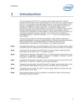
Introduction The 2nd Generation Intel® Core™ processor family mobile and Intel® Celeron® processor family mobile are the next generation of 64-bit, multi-core mobile processor built on 32- nanometer process technology. Based on a new micro-architecture, the processor is designed for a two-chip platform. The two-chip platform consists of a processor and Platform Controller Hub (PCH). The platform enables higher performance, lower cost, easier validation, and improved x-y footprint. The processor includes Integrated Display Engine, Processor Graphics and Integrated Memory Controller and is designed...
Open the catalog to page 11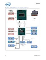
Figure 1-1. Mobile Platform System Block Diagram Example Discrete Graphics Embedded Display Intel* Flexible LVDS Flat Panel Network Connection
Open the catalog to page 12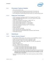
Processor Feature Details • Four or two execution cores • A 32-KB instruction and 32-KB data first-level cache (L1) for each core • A 256-KB shared instruction/data second-level cache (L2) for each core • Up to 8-MB shared instruction/data third-level cache (L3), shared among all cores Supported Technologies • Intel® Virtualization Technology (Intel® VT) for Directed I/O (Intel® VT-d) • Intel® Virtualization Technology (Intel® VT) for IA-32, Intel® 64 and Intel® Architecture (Intel® VT-x) • Intel® Active Management Technology 7.0 (Intel® AMT 7.0) • Intel® Trusted Execution Technology (Intel®...
Open the catalog to page 13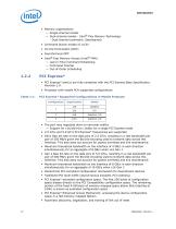
• Memory organizations — Single-channel modes — Dual-channel modes - Intel® Flex Memory Technology: - Dual-channel symmetric (Interleaved) • Command launch modes of 1n/2n • On-Die Termination (ODT) • Asynchronous ODT • Intel® Fast Memory Access (Intel® FMA) — Just-in-Time Command Scheduling — Command Overlap — Out-of-Order Scheduling PCI Express* • PCI Express* port(s) are fully-compliant with the PCI Express Base Specification, Revision 2.0. • Processor with mobile PCH supported configurations PCI Express* Supported Configurations in Mobile Products Configuration 1 • The port may negotiate down...
Open the catalog to page 14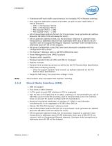
• Traditional AGP style traffic (asynchronous non-snooped, PCI-X Relaxed ordering) • Peer segment destination posted write traffic (no peer-to-peer read traffic) in Virtual Channel 0 — DMI -> PCI Express* Port 0 — DMI -> PCI Express* Port 1 — PCI Express* Port 0 -> DMI — PCI Express* Port 1 -> DMI • 64-bit downstream address format, but the processor never generates an address above 64 GB (Bits 63:36 will always be zeros) • 64-bit upstream address format, but the processor responds to upstream read transactions to addresses above 64 GB (addresses where any of Bits 63:36 are nonzero) with an Unsupported...
Open the catalog to page 15
• Supports the following traffic types to or from the PCH — DMI -> DRAM — DMI -> processor core (Virtual Legacy Wires (VLWs), Resetwarn, or MSIs only) — Processor core -> DMI • APIC and MSI interrupt messaging support — Message Signaled Interrupt (MSI and MSI-X) messages • Downstream SMI, SCI and SERR error indication • Legacy support for ISA regime protocol (PHOLD/PHOLDA) required for parallel port DMA, floppy drive, and LPC bus masters • DC coupling – no capacitors between the processor and the PCH • Polarity inversion • PCH end-to-end lane reversal across the link • Supports Half Swing “low-power/low-voltage”...
Open the catalog to page 16
Embedded DisplayPort* (eDP) • Stand alone dedicated port (unlike previous generation processor that shared pins with PCIe interface) Intel® Flexible Display Interface (Intel® FDI) • For SKUs with graphics, Intel FDI carries display traffic from the Processor Graphics in the processor to the legacy display connectors in the PCH • Based on DisplayPort standard • Two independent links – one for each display pipe • Four unidirectional downstream differential transmitter pairs — Scalable down to 3X, 2X, or 1X based on actual display bandwidth requirements — Fixed frequency 2.7 GT/s data rate • Two...
Open the catalog to page 17
Processor Graphics Controller • Intel® Rapid Memory Power Management (Intel® RMPM) – CxSR • Intel® Graphics Performance Modulation Technology (Intel® GPMT) • Intel Smart 2D Display Technology (Intel S2DDT) • Graphics Render C-State (RC6) • Intel Seamless Display Refresh Rate Switching with Embedded DisplayPort* Thermal Management Support • Digital Thermal Sensor • Intel Adaptive Thermal Monitor • THERMTRIP# and PROCHOT# support • On-Demand Mode • Open and Closed Loop Throttling • Memory Thermal Throttling • External Thermal Sensor (TS-on-DIMM and TS-on-Board) • Render Thermal Throttling • Fan...
Open the catalog to page 18All Intel catalogs and technical brochures
 10th Gen Intel® Core
7 Pages
 10th Gen
8 Pages
 nuc-celeron
4 Pages
 Intel® NUC 8 Home Mini PC
4 Pages
 Intel® Xeon® Scalable Platform
14 Pages
 Intel® Ethernet Controller XL710
1726 Pages
 Intel® Xeon® Processor E3-1200 v5
130 Pages
 Intel® Quark™ SoC X1000 Series
934 Pages
 Intel® X99 Chipset
4 Pages
 Intel® Desktop Board DQ67EP
4 Pages
 Intel® Ethernet Switch FM4000
270 Pages
 Intel® NUC Board DE3815TYBE
82 Pages
 S2600GZ and S2600GL
245 Pages
 i7-lga2011
314 Pages
 c600-series
936 Pages
 b75-express
4 Pages
 desktop-board
4 Pages
 3rd-gen-core-desktops
2 Pages
 /3rd-gen-core
2 Pages


Archived catalogs
 Intel® Ethernet Controllers
2 Pages
 Intel® 3450 Chipset
2 Pages
 Intel® 3000 and 3010 Chipset
4 Pages
 Intel® X58 Express Chipset
4 Pages
 Intel® Server Board S1200BT
8 Pages
 Intel® Desktop Board DX58SO2
4 Pages


- Management software solution
- Analysis software solution
- Real-time software
- Computer-aided design software
- Cloud-based software
- Design software solution
- Monitoring software solution
- Interface software
- Visualization software solution
- Simulation software solution
- Programming software
- Development software
- Network software
- Creation software
- Test software
- Wireless module
- Optimization software
- Solid-state drive
- Internal solid-state drive
- High-performance software