

2nd Gen Intel® Core? Processor Family Desktop Datasheet, Vol. 2

2nd Gen Intel® Core? Processor Family Desktop Datasheet, Vol. 2
This document is the second volume of the datasheet for the 2nd Generation Intel® Core™ Processor Family Desktop, Intel® Pentium® Processor Family Desktop, and Intel® Celeron® Processor Family Desktop. It provides detailed technical specifications and configuration information for these processors.
This section covers the configuration registers for processors, including register terminology, PCI devices and functions, and system address maps. It details various address ranges such as legacy, main memory, PCI memory, and graphics memory address ranges.
This section provides detailed information on the configuration registers for PCI devices, including Vendor Identification Register (VID), Device Identification Register (DID), PCI Command Register (PCICMD), PCI Status Register (PCISTS), and various Programmable Attribute Map Registers (PAM0-PAM6).
Details on SMM and VGA access through GTT TLB, and Intel® Management Engine (Intel ME) Stolen Memory Accesses are provided.
The document also discusses Intel® Trusted Execution Technology (Intel® TXT), Intel® Virtualization Technology, and Intel® Active Management Technology (Intel® AMT), highlighting the requirements and functionalities of these technologies.
The document includes legal disclaimers regarding the use of Intel products, emphasizing that the information is provided without any warranty and that Intel assumes no liability for its use. It also notes that the products may contain design defects or errors known as errata.
The processor supports various memory address ranges, including GMADR for graphics memory, and several programmable ranges such as PXPEPBAR, MCHBAR, and DMIBAR. These ranges must be unique and non-overlapping to ensure proper system functionality.
The document outlines the need for protected memory regions to secure MVMM code and data from unauthorized access. These regions are crucial for systems supporting Intel TXT and require proper configuration before launching MVMM.
This range is designed to protect memory from unauthorized DMA accesses, ensuring that only processor streams can access certain memory areas.
GSM is allocated for storing graphics translation table entries, and direct access to this space is restricted to hardware translations and fetches.
The document briefly mentions the allocation of UMA memory for Intel ME, which is "stolen" from the top of the host address space.
PCIEXBAR is located in device 0 configuration space. BIOS must assign this range to avoid conflicts. The processor can direct memory accesses to PCI Express interfaces using specified registers. Address decoding uses Memory Base and Limit Registers, aligning memory address ranges to 1 MB boundaries.
The processor does not support transactions that cross device boundaries, and PCI Express transactions are restricted from crossing a 4 KB boundary. Unsupported requests result in remapping to address 000C_0000h and dispatch to DRAM.
VC0 (Default) supports snoop and non-snoop asynchronous transactions. Internal Graphics GMADR writes occur without snooping. Peer writes and MSI are supported.
This document provides detailed information on processor configuration registers, focusing on access methods, reserved bits, and specific register functionalities.
Registers can be accessed in various sizes, with CONFIG_ADDRESS accessible only as a DWord. Multi-byte numeric fields use little-endian ordering. Registers in bytes 256 through 4095 require memory-mapped transactions in DWord quantities.
Reserved bits within registers must be handled carefully. On reads, software should mask out reserved bits, and on writes, preserve their values. Reserved address locations in the configuration space return zero on reads and have no effect on writes. Intel Reserved registers should not be modified as they may cause system failure.
Upon a full reset, configuration registers revert to default states, which represent minimum functionality. System initialization software, typically BIOS, must configure DRAM and other parameters for optimal performance.
The document outlines various registers related to the Integrated Graphics Device (IGD) and PCI devices. Key registers include the Maximum Latency Register (MAXLAT) and Multi Size Aperture Control Register (MSAC). The MAXLAT register has no specific latency timer settings required for the IGD, and it does not burst as a PCI compliant master. The MSAC register determines the size of the graphics memory aperture, which is set by the system BIOS and becomes read-only in a trusted environment.
The document describes the access methods for MMIO registers through the INDEX and DATA registers. The INDEX register is used to load the offset of the MMIO register, while the DATA register is used to read or write data to the specified MMIO location.
The document adheres to PCI standards for device identification and configuration. It specifies the Vendor Identification (VID) and Device Identification (DID) registers, which uniquely identify PCI devices. The PCI Command Register (PCICMD6) controls various device operations, including interrupt generation and error messaging.
System BIOS should save the MSAC register value on boot to ensure correct reset during S3 resume. The document also advises against using the MMIO access mechanism for VGA IO registers, which should be accessed directly through dedicated VGA IO ports.
The document includes tables listing register address maps and their attributes, such as access type, reset values, and descriptions. For example, the PCI Device 6 Register Address Map provides detailed information on each register's function and default settings.
Important parameters include the reset values and access types for each register, which dictate how they can be configured and used. Limitations are noted for certain registers, such as those hardwired to specific values or those that become read-only in a trusted environment.
Catalog excerpts

2nd Generation Intel® Core™ Processor Family Desktop, Intel® Pentium® Processor Family Desktop, and Intel® Celeron® Processor Family Desktop Datasheet, Volume 2 Supporting: Intel® Core™ i7, i5 and i3 Desktop Processor Series Intel® Pentium® G800 and G600 Desktop Processor Series Intel® Celeron® G500 and G400 Desktop Processor Series This is Volume 2 of 2
Open the catalog to page 1
INFORMATION IN THIS DOCUMENT IS PROVIDED IN CONNECTION WITH INTEL PRODUCTS. NO LICENSE, EXPRESS OR IMPLIED, BY ESTOPPEL OR OTHERWISE, TO ANY INTELLECTUAL PROPERTY RIGHTS IS GRANTED BY THIS DOCUMENT. EXCEPT AS PROVIDED IN INTEL'S TERMS AND CONDITIONS OF SALE FOR SUCH PRODUCTS, INTEL ASSUMES NO LIABILITY WHATSOEVER AND INTEL DISCLAIMS ANY EXPRESS OR IMPLIED WARRANTY, RELATING TO SALE AND/OR USE OF INTEL PRODUCTS INCLUDING LIABILITY OR WARRANTIES RELATING TO FITNESS FOR A PARTICULAR PURPOSE, MERCHANTABILITY, OR INFRINGEMENT OF ANY PATENT, COPYRIGHT OR OTHER INTELLECTUAL PROPERTY RIGHT. Legal Lines...
Open the catalog to page 2
Revision History Revision Number Revision Date January 2011 Initial release Added Intel® Pentium® processor family desktop Updated DSTS-Device Status Register (B/D/F/Type: 0/1/0/PCI) Added four registers to Section 2.13, MCHBAR Registers in Memory Controller – Channel 0. Added four registers to Section 2.14, MCHBAR Registers in Memory Controller – Channel 1 Added Intel® Celeron® processor family desktop
Open the catalog to page 10
Introduction This is Volume 2 of the Datasheet for the following products: • 2nd Generation Intel® Core™ processor family desktop • Intel® Pentium® processor family desktop • Intel® Celeron® processor family desktop The processor contains one or more PCI devices within a single physical component. The configuration registers for these devices are mapped as devices residing on the PCI Bus assigned for the processor socket. This document describes these configuration space registers or device-specific control and status registers (CSRs) only. This document does NOT include Model Specific Registers...
Open the catalog to page 11
Processor Configuration Registers Processor Configuration Registers This chapter contains the following: • Register terminology • PCI Devices and Functions on processor • System address map • Processor register introduction • Detailed register bit descriptions Register Terminology Table 2-1 shows the register-related terminology and register attributes that are used in this document. Attribute modifiers are listed in Table 2-2. Register Attributes and Terminology Item Read Only: These bits can only be read by software, writes have no effect. The value of the bits is determined by the hardware...
Open the catalog to page 13
Processor Configuration Registers Register Attribute Modifiers Attribute Modifier Applicable Attribute Sticky: These bits are only re-initialized to their default value by a "Power Good Reset". Note: Does not apply to RO (constant) bits. Key: These bits control the ability to write other bits (identified with a 'Lock' modifier) Lock: Hardware can make these bits "Read Only" via a separate configuration bit or other logic. Note: Mutually exclusive with 'Once' modifier. Once: After reset, these bits can only be written by software once, after which they become "Read Only". Note: Mutually exclusive...
Open the catalog to page 14
Processor Configuration Registers System Address Map The processor supports 512 GB (39 bit) of addressable memory space and 64 KB+3 of addressable I/O space. This section focuses on how the memory space is partitioned and what the separate memory regions are used for. I/O address space has simpler mapping and is explained near the end of this section. The processor supports PEG port upper prefetchable base/limit registers. This allows the PEG unit to claim I/O accesses above 32 bit. Addressing of greater than 4 GB is allowed on either the DMI Interface or PCI Express interface. The processor...
Open the catalog to page 15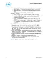
Processor Configuration Registers • Device 6, Function 0 — MBASE/MLIMIT – PCI Express port non-prefetchable memory access window. — PMBASE/PMLIMIT – PCI Express port prefetchable memory access window. — PMUBASE/PMULIMIT – PCI Express port upper prefetchable memory access window — IOBASE/IOLIMIT – PCI Express port I/O access window. • Device 2, Function 0 — IOBAR – I/O access window for internal graphics. Through this window address/data register pair, using I/O semantics, the IGD and internal graphics instruction port registers can be accessed. Note, this allows accessing the same registers as...
Open the catalog to page 16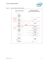
Processor Configuration Registers System Address Range Example PHYSICAL MEMORY (DRAM CONTROLLER VIEW) HOST/SYSTEM VIEW 512 GB PCI Memory Add. Range TOUUD BASE Reclaim Limit = Reclaim Base + x 1 MB aligned Reclaim BASE Main Memory Reclaim Add Range ME-UMA MESEG BASE Main memory Address Range Flash, APIC Intel TXT (20 MB) TSEG TSEG BASE Main Memory Add Range
Open the catalog to page 17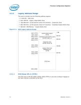
Processor Configuration Registers Legacy Address Range This area is divided into the following address regions: • 0–640 KB – DOS Area • 640–768 KB – Legacy Video Buffer Area • 768–896 KB in 16 KB sections (total of 8 sections) – Expansion Area • 896–960 KB in 16 KB sections (total of 4 sections) – Extended System BIOS Area • 960 KB–1 MB Memory – System BIOS Area DOS Legacy Address Range 000F_FFFFh 000F_0000h 000E_FFFFh 000E_0000h System BIOS (Upper) 64 KB Extended System BIOS (Lower) 64 KB (16 KB x 4) 000B_FFFFh Legacy Video Area (SMM Memory) 128 KB 000A_0000h 0009_FFFFh DOS Range (0h–9_FFFFh)...
Open the catalog to page 18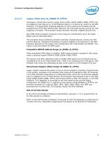
Processor Configuration Registers Legacy Video Area (A_0000h–B_FFFFh) The legacy 128 KB VGA memory range, frame buffer, (000A_0000h–000B_FFFFh) can be mapped to IGD (Device 2), to PCI Express (Device 1 or Device 6), and/or to the DMI Interface. The appropriate mapping depends on which devices are enabled and the programming of the VGA steering bits. Based on the VGA steering bits, priority for VGA mapping is constant. The processor always decodes internally mapped devices first. Non-SMM-mode processor accesses to this range are considered to be to the Video Buffer Area as described above. The...
Open the catalog to page 19All Intel catalogs and technical brochures
 10th Gen Intel® Core
7 Pages
 10th Gen
8 Pages
 nuc-celeron
4 Pages
 Intel® NUC 8 Home Mini PC
4 Pages
 Intel® Xeon® Scalable Platform
14 Pages
 Intel® Ethernet Controller XL710
1726 Pages
 Intel® Xeon® Processor E3-1200 v5
130 Pages
 Intel® Quark™ SoC X1000 Series
934 Pages
 Intel® X99 Chipset
4 Pages
 Intel® Desktop Board DQ67EP
4 Pages
 Intel® Ethernet Switch FM4000
270 Pages
 Intel® NUC Board DE3815TYBE
82 Pages
 S2600GZ and S2600GL
245 Pages
 i7-lga2011
314 Pages
 c600-series
936 Pages
 b75-express
4 Pages
 desktop-board
4 Pages
 3rd-gen-core-desktops
2 Pages
 /3rd-gen-core
2 Pages


Archived catalogs
 Intel® Ethernet Controllers
2 Pages
 Intel® 3450 Chipset
2 Pages
 Intel® 3000 and 3010 Chipset
4 Pages
 Intel® X58 Express Chipset
4 Pages
 Intel® Server Board S1200BT
8 Pages
 Intel® Desktop Board DX58SO2
4 Pages


- Management software solution
- Analysis software solution
- Real-time software
- Computer-aided design software
- Cloud-based software
- Design software solution
- Monitoring software solution
- Interface software
- Visualization software solution
- Simulation software solution
- Programming software
- Development software
- Network software
- Creation software
- Test software
- Wireless module
- Optimization software
- Solid-state drive
- Internal solid-state drive
- High-performance software