- Catalogs
- Infineon Technologies AG
- RF & Protection Devices Selection Guide
- Products
- Catalogs
- News & Trends
- Exhibitions
RF & Protection Devices Selection Guide
1 /60Pages

RF & Protection Devices Selection Guide
1 /60Pages
Catalog excerpts

RF & Protection Devices Selection Guide
Open the catalog to page 1
General Purpose LNAs 5 Antenna Switch Module 6 General Purpose Switches 6 Antenna Aperture Tuning RF Switches 6 Ultra Low Noise SiGe:C Transistors for use 7 High Linearity Si- and SiGe:C-Transistors for use 8 Biased Low Noise RF Transistor 8 Single Full Biased 9 Single Semi Biased 9 Dual Semi Biased 9 Band Switching and RF Attenuation 10 RF Mixer + Detector Schottky Diode 14 Surge Protection Devices 18 Alphanumerical List of the Symbols used 20
Open the catalog to page 3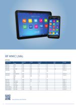
RF MMIC LNAs LTE LNAs Product Type
Open the catalog to page 4
GNSS LNAs Product Type General Purpose LNAs Product Type Application notes, Data sheets, Simulation data: www.infineon.com/rfmmic.documents RF Modules Navigation Rx Front-End Product Type Product information: www.infineon.com/rfmodule
Open the catalog to page 5
RF Switches Antenna Switch Module Product Type Switch Type Control Interface MIPI RFFE Diversity Switches Product Type Switch Type Control Interface MIPI RFFE MIPI RFFE General Purpose Switches Product Type Switch Type Control Interface Application notes, Data sheets, Simulation data: www.infineon.com/rfswitches.documents Antenna Tuning Antenna Aperture Tuning RF Switches Product Type Product information: www.infineon.com/rfswitches
Open the catalog to page 6
RF Transistors Low Noise Si Transistors up to 2.5GHz Product Type High Gain up to 2.5GHz, Flatlead TSFP Package Respectively TSLP Package for Modules BFR340F Low Noise Si Transistors up to 5GHz Product Type For Modules in TSLP Package BFR460L3 Ultra Low Noise SiGe:C Transistors for use up to 12GHz Product Type Robust Low Noise Broadband Pre-Matched SiGe:C Transistors BFP843F
Open the catalog to page 7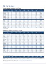
RF Transistors Ultra Low Noise SiGe:C Transistors for use up to 12GHz Product Type High Linearity Si- and SiGe:C-Transistors for use up to 6GHz Product Type VCEO (max) IC (max) [V] [mA] For Low Frequencies, e.g. VHF/UHF Biased Low Noise RF Transistor Product Type Application notes, Data sheets, Simulation data: www.infineon.com/rftransistors.documents
Open the catalog to page 8
RF MOSFET Single Full Biased Product Type Single Non Biased Product Type Single Semi Biased Product Type Dual Semi Biased Product Type Application notes, Data sheets, Simulation data: www.infineon.com/rfmosfet.documents
Open the catalog to page 9
RF Pin Diode Band Switching and RF Attenuation Product Type
Open the catalog to page 10
Antenna Switch Product Type 1) Not for new design 2) Typical value 3) On request Application notes, Data sheets, Simulation data: www.infineon.com/pindiodes.documents
Open the catalog to page 11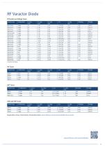
RF Varactor Diode VCO and Low Voltage Tuner Product Type Product Type SAT Tuner Product Type UHF and VHF Tuner Product Type Application notes, Data sheets, Simulation data: www.infineon.com/varactordiodes.documents
Open the catalog to page 13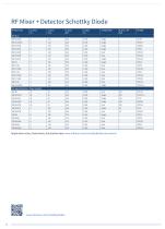
RF Mixer + Detector Schottky Diode Product Type RF Signal Detection + Power Leveling BAT62 Application notes, Data sheets, Simulation data: www.infineon.com/schottkydiodes.documents
Open the catalog to page 14
RF mmW-MMIC 24GHz Industrial Product Type Frequency Divider Temperatur Sensor Backhaul Product Type Power Detector Temperatur Sensor Application notes, Data sheets, Simulation data: www.infineon.com/mmWave.documents
Open the catalog to page 15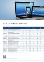
ESD & EMI Protection and Filters Multi-Purpose ESD Devices Product Type keypad, touchscreen, buttons, convenience keys, audio keypad, touchscreen, buttons, Audio keypad, touchscreen, buttons, Audio Audio Line, Speaker, Headset, Microphone Protection, Human Interface Devices Audio Line, Speaker, Headset, Microphone Protection, Human Interface Devices keypad, touchscreen, buttons, convenience keys keypad, touchscreen, buttons, convenience keys keypad, touchpad, buttons, convenience keys keypad, touchpad, buttons, convenience keys Audio Line, Speaker, Headset, Microphone Protection, Human Interface...
Open the catalog to page 16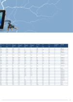
RDYN,typ reverse RDYN,typ forward Protected Lines
Open the catalog to page 17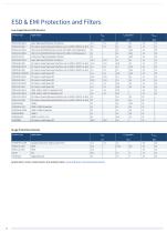
Application notes, Data sheets, Simulation data: www.infineon.com/esd.documents
Open the catalog to page 18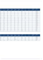
RDYN,typ reverse RDYN,typ forward Protected Lines RDYN,typ reverse RDYN,typ forward Protected Lines
Open the catalog to page 19
Alphanumerical List of the Symbols used Symbols Output 3rd-order intercept point Output capacitance Power output at -1dB compression point Line capacitance Maximum power Saturation power Total diode capacitance Total power dissipation Electrostatic discharge Transmitter power Noise factor RDYN,typ forward Forward dynamic resistance RDYN,typ reverse Reverse dynamic resistance Transition frequency Forward resistance of diodes Forward transconductance Differential resistance Power gain Series resistance Receiver gain Collector current (DC or average value) Charge carrier life time Transmitter current...
Open the catalog to page 20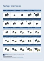
All products are available in green (RoHS compliant). Footprints are recommendations only. For detailed information please refer to our datasheets or www.infineon.com/packages.
Open the catalog to page 22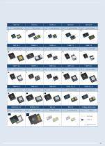
Package (JEITA-code)
Open the catalog to page 23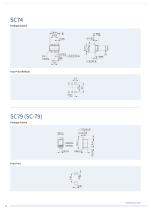
Foot Print (Reflow) Cathode marking Foot Print
Open the catalog to page 24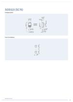
Foot Print (Reflow)
Open the catalog to page 25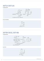
Package Outline 1.9 1) Lead width can be 0.6 max. in dambar area Foot Print (Reflow) 1) Ejector pin markings possible Foot Print
Open the catalog to page 26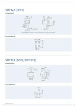
Package Outline Note: Mold flash, protrusions or gate burrs of 0,2 mm max. per side are not included Foot Print (Reflow) Foot Print (Reflow)
Open the catalog to page 27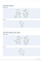
Foot Print Foot Print
Open the catalog to page 28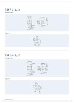
Foot Print Foot Print
Open the catalog to page 29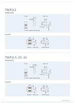
TSLP-2-1 Package Outline Top view Cathode marking 1) Dimension applies to plated terminals Foot Print Solder mask Stencil apertures TSLP-2-7, -17, -21 Package Outline Bottom view Cathode marking 1) Dimension applies to plated terminals Solder mask Foot Print Stencil apertures
Open the catalog to page 30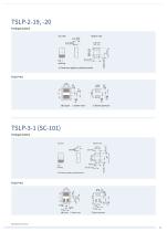
TSLP-2-19, -20 Package Outline Bottom view 1) Dimension applies to plated terminals Foot Print Solder mask Stencil apertures TSLP-3-1 (SC-101) Package Outline Bottom view 1) Dimension applies to plated terminal Foot Print Stencil apertures
Open the catalog to page 31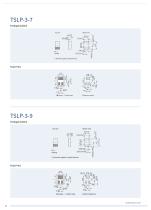
TSLP-3-7 Package Outline Bottom view 1) Dimension applies to plated terminal Foot Print Solder mask Stencil apertures TSLP-3-9 Package Outline Top view Bottom view 1) Dimension applies to plated terminal Solder mask Foot Print Stencil apertures
Open the catalog to page 32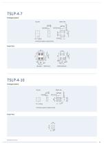
Pin 1 marking 1) Dimension applies to plated terminal Stencil apertures Solder mask 1) Dimension applies to plated terminals Foot Print
Open the catalog to page 33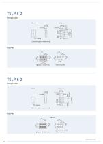
TSLP-5-2 Package Outline Bottom view +0.01 Pin 1 marking 1) Dimension applies to plated terminals Stencil apertures Solder mask TSLP-6-2 Package Outline Top view Bottom view 1) Dimension applies to plated terminals Foot Print NSMD (stencil thickness 100 µm) Copper Solder mask Stencil apertures
Open the catalog to page 34All Infineon Technologies AG catalogs and technical brochures
 IPB60R045P7
14 Pages
 IPD900P06NM
10 Pages
 Every switch needs a driver
10 Pages
 CoolMOS™ 7 - CoolSiC™ - CoolGaN™
28 Pages
 IPAN60R360P7S
14 Pages
 IPAN60R180P7S
14 Pages
 IPP60R160P7
14 Pages
 IPZA60R045P7
14 Pages
 BSZ063N04LS6
11 Pages
 BAW78.../BAW79...
6 Pages
 Automotive Power Selection Guide
114 Pages
 Custom Made Blanking Line
9 Pages
 XC800 Family
54 Pages
 IFBIP-Company-Brochure
11 Pages
 Shortform Catalog 2013
212 Pages
 Efficient Lighting Brochure 2013
24 Pages
 Industrial Automation Brochure
52 Pages
 Transceiver Brochure
16 Pages
 Automotive Application Guide
54 Pages
 ESD/Surge Protection Diodes
43 Pages
 IGBT Selection Guide
6 Pages
 Payment
5 Pages
 Absolute Pressure Sensor
24 Pages
 Schottky Diodes
7 Pages
 Silicon Switching Diode
6 Pages
 Dual Ic
8 Pages
 PrimePACK™ IGBT Modules
2 Pages


Archived catalogs
 Linear Voltage Regulators
17 Pages
 ModSTACK™ HD
2 Pages
 8-Bit Microcontrollers
20 Pages
 Sense & Control Selection Guide
24 Pages
 Communication Brochure
8 Pages
 COM Image Brochure
12 Pages


- AMOT power supply
- AMOT DC power supply
- AMOT AC/DC power supply
- Switching power supply
- DC-DC converter
- Regulated power supply
- Industrial DC/DC converter module
- SMD DC-DC converter
- AMOT magnetic sensor
- Open frame power supply
- AMOT switching transistor
- CE DC/DC converter module
- AMOT MOSFET transistor
- Current rectifier
- Bipolar transistor
- AMOT microcontroller
- Switching DC-DC converter
- Hall effect magnetic sensor
- Development kit