- Catalogs
- Infineon Technologies AG
- Linear Voltage Regulators
- Products
- Catalogs
- News & Trends
- Exhibitions
Linear Voltage Regulators
1 /17Pages

Linear Voltage Regulators
1 /17Pages
Catalog excerpts
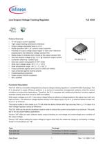
Feature Overview 70 mA output current capabilityՕTight output tracking tolerance to referenceOutput voltage adjustable down to 2.0 V ՕStable operation with 1 F ceramic output capacitorՕFlexibility of output voltage adjust higher or lower than reference, proportional to the reference voltage (version GA)Status output to indicate short circuits at the output (version GS)ՕVery low dropout voltage of typ. 0.2 V @ maximum output currentCombined reference / enable inputՕVery low current consumption in OFF mode Wide input voltage range -20 V բɤ PG-DSO-8-10 > I ≤ +45 VWide temperature range: -40 հC ≤ > j ≤ 150 CЕOutput protected against short circuit to GND and batteryInput protected against reverse polarityՕOvertemperature protectionGreen product (RoHS compliant) ՕAEC qualified Functional Description The TLE4254 is a monolithic integrated low-dropout voltage tracking regulator in a small PG-DSO-8 package. TheIC is designed to supply off-board systems, e.g. sensors in powertrain management systems under the severeconditions of automotive applications. Therefore, the IC is equipped with additional protection functions againstreverese polarity and short circuit to GND and battery.With supply voltages up to 40V, the output voltage follows a reference voltage applied at the adjust input with veryhigh accuracy. The reference voltage applied directly to the adjust input or by an e.g. external resistor divider canbe 2.0V at minimum. The output is able to drive loads up to 70 mA while the device follows with high accuracy the e.g. 5V output of amain voltage regulator acting as reference.The TLE4254 can be set into shutdown mode in order to reduce the current consumption to a minimum. This suitsthe IC for low power battery applications.Version GSӔ offers an open collector status output indicating an overvoltage and undervoltage error condition ofthe output voltage.Version GAӔ allows setting the output voltage to higher value than the reference voltage by connecting a voltagedivider to the feedback pin FBӔ. TypePackage TLE4254GA PG-DSO-8-10 (RoHS compliant) TLE4254GS PG-DSO-8-10 (RoHS compliant) Data Sheet 1Rev. 1.0, 2006-11-22 >
Open the catalog to page 1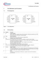
GND56 78 GNDGND GNDFBEN/ADJI GNDGND GNDSTEN/ADJI Figure1Pin Configurations > PinSymbolFunction 1Q Tracker Output. Block to GND with a capacitor close to the IC terminals, respecting capacitance and ESR requirements given in the table Functional RangeӔ.2, 3, 6, 7GND Ground reference. Interconnect the pins on PCB. Connect to heatsink area.4FB(version GA) Feedback input (version GA only). Non inverting input of the internal error amplifier to control the output voltage.Connect this pin directly to the output pin in order to obtain lower or equal output voltages with respect to the reference voltage....
Open the catalog to page 2
tr.row {} td.cell {} div.block {} div.paragraph {}
Open the catalog to page 3
General Product Characteristics > Pos.ParameterSymbolLimit ValuesUnitConditionsMin.Max. 2.2.1Input Voltage > dr 2.2.1Adjust / Enable Input Voltage (Voltage Tracking Range) > 1) CQ ֖5 Ω > 1)Not subject to production test; specified by design. Note:Within the functional range the IC operates as described in the circuit description. The electrical characteristics are specified within the conditions given in the related electrical characteristics table. > Pos.ParameterSymbolTyp. ValueUnitConditions PG-DSO-8-10: 2.3.1Junction ֖ Ambient > 1) 2) th,j-a 155K/WFootprint only 2.3.296K/W300 mm > 2 PCB heatsink...
Open the catalog to page 4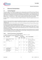
Q is controlled by comparing it to the voltage applied at pin ADJ/EN and driving a PNP passtransistor accordingly. The control loop stability depends on the output capacitor > Q , the load current, the chiptemperature and the poles/zeros introduced by the integrated circuit and the load. To ensure stable operation, theoutput capacitors capacitance and its equivalent series resistor ESR requirements given in the table ғFunctionalRange have to be maintained. For details see also the typical performance graph ԓOutput Capacitor SeriesResistor > Q . Also, the output capacitor shall be sized to buffer...
Open the catalog to page 5
Electrical Characteristics Table1Electrical Characteristics Tracking Regulator > Q = 1 еF; all voltages with respect to ground (unless otherwise specified). Pos.ParameterSymbolLimit ValuesUnitTest ConditionMin.Typ.Max. 3.1.6Power Supply Ripple Rejection > 1) Q = 10 F, ceramic type 3.1.7Dropout Voltage > ADJ/EN = 5 V3.1.10Reverse Current at Negative Input Voltage > ADJ/EN = 5 V Feedback Input FB (version GA only): 3.1.11Feedback Input Biasing Current > FB = 5 V Overtemperature Protection: 3.1.12Junction Temperature Equilibrium > j increasing due to power dissipation generated by the IC > 1) 1)Parameter...
Open the catalog to page 6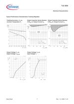
VQ-VADJ.vsd VQ-VI.vsd
Open the catalog to page 7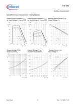
Vdr-IQ_log.vsd Vdr-Tj.vsd +1 > II-VI.vsd
Open the catalog to page 8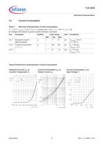
tr.row {} td.cell {} div.block {} div.paragraph {}
Open the catalog to page 9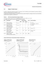
In order to reduce the quiescent current to a minumum, the TLE4254G can be switched to stand-by mode bysetting the adjust/enable input ADJ/ENӔ to lowӔ.In case the pin ADJ/EN is left open, an internal pull-down resistors keeps the voltage at the pin low and thereforeensures that the regulator is switched off. Table3Electrical Characteristics Adjust / Enable > Q = 1 еFall voltages with respect to ground (unless otherwise specified). Pos.ParameterSymbolLimit ValuesUnitTest ConditionMin.Typ.Max. 3.3.1Adjust / Enable Low Signal Valid > j բɤ 125 C3.3.2Adjust / Enable High Signal Valid (Tracking Region)...
Open the catalog to page 10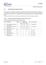
The status output ST indicates an overvoltage or undervoltage situation at the regulators output Q. Therefore, theoutput voltage > Q is compared to the reference voltage > ADJ/EN . Variations of the output voltage are indicated bya low signal at the status output ST. Transients shorter than the status reaction time > ST,r will not trigger the statusoutput.The status output ST is an open collector output, requiring a pull-up resisitor to a positive voltage rail. Table4Electrical Characteristics Status Output ST (Version GS only) > Q = 1 еFall voltages with respect to ground (unless otherwise specified)....
Open the catalog to page 11All Infineon Technologies AG catalogs and technical brochures
 IPB60R045P7
14 Pages
 IPD900P06NM
10 Pages
 Every switch needs a driver
10 Pages
 CoolMOS™ 7 - CoolSiC™ - CoolGaN™
28 Pages
 IPAN60R360P7S
14 Pages
 IPAN60R180P7S
14 Pages
 IPP60R160P7
14 Pages
 IPZA60R045P7
14 Pages
 BSZ063N04LS6
11 Pages
 BAW78.../BAW79...
6 Pages
 Automotive Power Selection Guide
114 Pages
 Custom Made Blanking Line
9 Pages
 XC800 Family
54 Pages
 IFBIP-Company-Brochure
11 Pages
 Shortform Catalog 2013
212 Pages
 Efficient Lighting Brochure 2013
24 Pages
 Industrial Automation Brochure
52 Pages
 Transceiver Brochure
16 Pages
 Automotive Application Guide
54 Pages
 ESD/Surge Protection Diodes
43 Pages
 IGBT Selection Guide
6 Pages
 Payment
5 Pages
 Absolute Pressure Sensor
24 Pages
 Schottky Diodes
7 Pages
 Silicon Switching Diode
6 Pages
 Dual Ic
8 Pages
 PrimePACK™ IGBT Modules
2 Pages


Archived catalogs
 ModSTACK™ HD
2 Pages
 8-Bit Microcontrollers
20 Pages
 Sense & Control Selection Guide
24 Pages
 Communication Brochure
8 Pages
 COM Image Brochure
12 Pages


- Power supply unit
- DC power supply
- AC/DC power supply
- Switching power supply
- Single-output power supply
- DC-DC converter
- Regulated power supply
- Infineon transistor
- Industrial DC/DC converter module
- SMD DC-DC converter
- Open frame power supply
- Infineon switching transistor
- CE DC/DC converter module
- Infineon MOSFET transistor
- Current rectifier
- Bipolar transistor
- Microcontroller
- Switching DC-DC converter
- Development kit
- Industrial AC/DC converter