
Catalog excerpts

MOSFET OptiMOSTM6 Power-Transistor, 40 V Features • Optimized for synchronous application • Very low on-resistance ^DS(on) • 100% avalanche tested • Superior thermal resistance • N-channel • Qualified according to JEDEC1) for target applications • Pb-free lead plating; RoHS compliant • Halogen-free according to IEC61249-2-21 • 175 °C rated Table 1 Key Performance Parameters Type / Ordering Code 1) J-STD20 and JESD22 Final Data Sheet
Open the catalog to page 1
TableofContents Description . . . . . . . . . . . . . . . . . . . . . . . . . . . . . . . . . . . . . . . . . . . . . . . . . . . . . . . . . . . . . . . . . . . . . . . . . . . . . 1 Maximum ratings . . . . . . . . . . . . . . . . . . . . . . . . . . . . . . . . . . . . . . . . . . . . . . . . . . . . . . . . . . . . . . . . . . . . . . . . 3 Thermal characteristics . . . . . . . . . . . . . . . . . . . . . . . . . . . . . . . . . . . . . . . . . . . . . . . . . . . . . . . . . . . . . . . . . . . . 3 Electrical characteristics . . . . . . . . . . . . . . . . . . . . . . . . . . . . . . ....
Open the catalog to page 2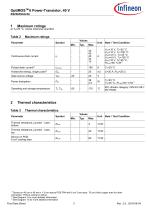
at Ta=25 °C, unless otherwise specified Table 2 Maximum ratings Note / Test Condition Continuous drain current Avalanche energy, single pulse3 Gate source voltage Power dissipation Operating and storage temperature 2 Thermal characteristics Table 3 Thermal characteristics 11 Device on 40 mm x 40 mm x 1.5 mm epoxy PCB FR4 with 6 cm2 (one layer, 70 pm thick) copper area for drain connection. PCB is vertical in still air. 2) See Diagram 3 for more detailed information 3) See Diagram 13 for more detailed information Final Data Sheet
Open the catalog to page 3
at 7]=25 °C, unless otherwise specified Table 4 Static characteristics 11 Defined by design. Not subject to production test. 2) See "Gate charge waveforms" for parameter definition Final Data Sheet
Open the catalog to page 4
Table 7 Reverse diode 11 Defined by design. Not subject to production test. Final Data Sheet
Open the catalog to page 5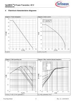
Diagram 2: Drain current Diagram 3: Safe operating area Diagram 4: Max. transient thermal impedance 103 tp [s] Zthjc=f(fp); parameter: D=fp/T Final Data Sheet
Open the catalog to page 6
Diagram 5: Typ. output characteristics Diagram 6: Typ. drain-source on resistance Final Data Sheet Rev. 2.0, 2018-06-04
Open the catalog to page 7
Diagram 9: Normalized drain-source on resistance Diagram 10: Typ. gate threshold voltage _Tj_[°C]_ /GS(th=f(Tj), /gs=/ds; parameter: Id Diagram 12: Forward characteristics of reverse diode Final Data Sheet
Open the catalog to page 8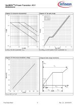
Diagram Gate charge waveforms Final Data Sheet
Open the catalog to page 9
Figure 1 Outline PG-TSDSON-8 FL, dimensions in mm/inches Final Data Sheet
Open the catalog to page 10
OptiMOS™ 6 Power-Transistor, 40 VBSZ063N04LS6Revision History BSZ063N04LS6 Revision: 2018-06-04, Rev. 2.0Previous Revision Revision Trademarks All referenced product or service names and trademarks are the property of their respective owners. We Listen to Your Comments Any information within this document that you feel is wrong, unclear or missing at all? Your feedback will help us to continuously improve the quality of this document. Please send your proposal (including a reference to this document) to: erratum@infineon.com Published by Infineon Technologies AG 81726 Munchen, Germany ©...
Open the catalog to page 11All Infineon Technologies AG catalogs and technical brochures
-
IPB60R045P7
14 Pages
-
IPD900P06NM
10 Pages
-
Every switch needs a driver
10 Pages
-
CoolMOS™ 7 - CoolSiC™ - CoolGaN™
28 Pages
-
IPAN60R360P7S
14 Pages
-
IPAN60R180P7S
14 Pages
-
IPP60R160P7
14 Pages
-
IPZA60R045P7
14 Pages
-
BAW78.../BAW79...
6 Pages
-
Automotive Power Selection Guide
114 Pages
-
Custom Made Blanking Line
9 Pages
-
XC800 Family
54 Pages
-
IFBIP-Company-Brochure
11 Pages
-
Shortform Catalog 2013
212 Pages
-
Efficient Lighting Brochure 2013
24 Pages
-
Industrial Automation Brochure
52 Pages
-
Transceiver Brochure
16 Pages
-
Automotive Application Guide
54 Pages
-
ESD/Surge Protection Diodes
43 Pages
-
IGBT Selection Guide
6 Pages
-
Payment
5 Pages
-
Absolute Pressure Sensor
24 Pages
-
Schottky Diodes
7 Pages
-
Silicon Switching Diode
6 Pages
-
Dual Ic
8 Pages
-
PrimePACK™ IGBT Modules
2 Pages
Archived catalogs
-
Linear Voltage Regulators
17 Pages
-
ModSTACK™ HD
2 Pages
-
8-Bit Microcontrollers
20 Pages
-
Sense & Control Selection Guide
24 Pages
-
Communication Brochure
8 Pages
-
COM Image Brochure
12 Pages


