

MT9P031

MT9P031
- 1/2.5-Inch 5Mp CMOS Digital Image Sensor with high frame rate and superior low-light performance.
- Global reset release for simultaneous exposure of all rows and bulb exposure mode for arbitrary exposure times.
- Snapshot mode, horizontal and vertical mirror image, and column/row skip and binning modes for image size and quality adjustments.
- Simple two-wire serial interface with programmable controls for gain, frame rate, frame size, and exposure.
- Automatic black level calibration and on-chip phase-locked loop (PLL).
- High-resolution network cameras, wide FOV cameras, 720P–60 fps cameras, dome cameras with electronic pan, tilt, and zoom.
- Hybrid video cameras with high-resolution stills and smart cameras for detailed feature extraction.
Available in various configurations including 48-pin iLCC and demo headboard versions.
The MT9P031 is a 1/2.5-inch CMOS active-pixel digital image sensor with a 2592H x 1944V pixel array. It includes advanced camera functions like windowing and snapshot mode, programmable via a two-wire serial interface.
- Optical format: 1/2.5-inch (4:3), Active imager size: 5.70mm x 4.28mm, 7.13mm diagonal.
- Pixel size: 2.2 x 2.2μm, Color filter array: RGB Bayer pattern.
- Shutter type: Global reset release and electronic rolling shutter.
- Maximum data rate: 96 Mp/s at 96 MHz, Frame rate: Up to 14 fps full resolution, 53 fps VGA with binning.
- ADC resolution: 12-bit, Responsivity: 1.4 V/lux-sec, Pixel dynamic range: 70.1dB, SNRMAX: 38.1dB.
- Supply Voltage: I/O 1.7–3.1V, Digital 1.7–1.9V, Analog 2.6–3.1V, Power consumption: 381mW at 14 fps full resolution.
- Operating temperature: –30°C to +70°C, Packaging: 48-pin iLCC, die.
The sensor is a progressive-scan type that generates pixel data at a constant frame rate. It uses an on-chip PLL to generate internal clocks from a master input clock ranging from 6 to 27 MHz, with a maximum pixel rate of 96 Mp/s. The sensor's core is a 5Mp active-pixel array, and it uses a two-wire serial bus for user interaction. The pixel data is processed through an analog signal chain and an ADC, outputting a 12-bit value for each pixel.
The pixel array consists of a 2752-column by 2004-row matrix, with a 2592-column by 1944-row active region in the center. This structure allows for a default output image surrounded by a boundary region and a border of dark pixels, which can be used for monitoring black levels.
The document details various electrical specifications, including the two-wire serial register interface, I/O timing, and DC electrical characteristics. It also includes information on power consumption and absolute maximum ratings.
The sensor is housed in a 48-pin iLCC package, with detailed pin descriptions provided. The package dimensions and pinout diagrams are included for reference.
The document contains numerous figures and tables illustrating block diagrams, typical configurations, pixel array descriptions, and timing diagrams. Key tables include available part numbers, key performance parameters, and operating modes.
The MT9P031 is a 1/2.5-inch 5Mp digital image sensor. It operates with a digital supply voltage of 1.8V and an IO supply voltage of either 1.8V or 2.8V. The analog supply voltage is nominally 2.8V. The sensor outputs pixel data in a Bayer pattern format with four colors: GreenR, GreenB, Red, and Blue. The pixel array consists of active and dark pixels, with specific columns and rows designated for each type.
The sensor outputs data in a progressive scan format, with valid image data surrounded by horizontal and vertical blanking. The default readout order starts from pixel (16, 54). The pixel array is read out one row at a time, with specific sequences for dark and active pixels.
The output images are divided into frames and lines, with signals FV and LV indicating frame and line boundaries. The sensor outputs one 12-bit pixel datum per PIXCLK cycle. The timing of FV and LV is related to row and frame time, with options for continuous LV assertion.
The frame time is determined by the pixel clock and is influenced by horizontal and vertical blanking. The document provides equations for calculating frame time and examples of frame rates at common resolutions, both with and without subsampling.
The MT9P031 uses a two-wire serial interface for register read and write operations. The protocol involves start and stop bits, an 8-bit slave address, and data transfer in 8-bit increments. The bus is idle when both data and clock lines are high, and control is initiated with a start bit.
Data is transferred 8 bits at a time with an acknowledge bit. The master generates the clock pulse, and data must be stable during the HIGH period of the clock. Acknowledge and no-acknowledge bits are used to manage data transfer sequences.
The document describes 16-bit WRITE and READ sequences. A WRITE sequence involves sending a start bit, write address, register address, and 16-bit data, with acknowledge bits after each 8-bit transfer. A READ sequence involves writing the register address, followed by a start bit and read address, with data being clocked out 8 bits at a time.
The sensor can be reset using a hard reset (RESET_BAR) or a soft reset via the reset register. Hard reset returns all registers to factory defaults, while soft reset retains certain settings.
The power-up sequence involves asserting RESET_BAR, bringing up supplies, and negating RESET_BAR. Power down requires asserting RESET_BAR before removing supplies.
The sensor requires an EXTCLK, nominally 96 MHz. The clock can be divided internally, and a PLL can generate the pixel clock. The PLL setup involves configuring divisors to achieve desired frequencies.
The sensor can enter a low-power standby state via hard or soft methods. In standby, internal clocks are gated, and analog circuitry minimizes power draw. The sensor resumes from its previous state upon exiting standby.
The entire array, including dark pixels, can be read without digital processing. Specific register settings control the readout configuration.
The output image window is defined by register fields for start coordinates and size. The document specifies conditions for setting these fields.
Subsampling and binning reduce output resolution. Skipping involves not sampling certain rows/columns, while binning combines adjacent pixels. Legal combinations of binning and skipping are provided.
The document describes how to reverse the readout order of rows and columns, preserving the Bayer pattern.
The sensor allows for pixel readout direction reversal, affecting only active region pixels. When combined with row or column mirroring, binning is performed in the positive direction. This affects the order and averaging of pixel rows during readout.
Maintaining a constant frame rate is challenging due to synchronization requirements between register updates and readout pointers. Certain register fields can cause a temporary increase in vertical blanking, affecting output rate.
Changes to register fields affecting image size or brightness take effect on the subsequent frame. Special provisions allow for immediate effect in snapshot modes under certain conditions.
The sensor can be restarted at any time, interrupting the current frame and applying register updates immediately. The Pause_Restart feature allows for controlled timing of frame initiation.
The sensor supports Electronic Rolling Shutter (ERS) and Global Reset Release (GRR) modes. ERS involves sequential row scanning, while GRR starts exposure simultaneously for all rows, reducing motion shear.
Exposure time is calculated based on shutter width and delay parameters. In GRR modes, exposure starts simultaneously for all rows, typically controlled by an external shutter.
The sensor operates in continuous or snapshot modes, with exposure controlled electronically or via external triggers. Various modes are detailed, including ERS and GRR snapshot and bulb modes.
The sensor provides a STROBE output for synchronizing exposure with external events. The timing of the strobe signal can be configured to align with specific exposure phases.
The document outlines the signal processing chain, highlighting independent processing for each color channel, including gain and offset adjustments.
The document describes the signal processing path of the MT9P031 digital image sensor, which includes both analog and digital gain stages. The analog gain can be adjusted between 1 and 8, while the digital gain ranges from 1 to 16. The combined gain can reach up to 128. The analog offset is automatically determined by a black level calibration algorithm, while the digital offset is used for fine-tuning.
The document provides recommended gain settings and explains that analog gain should be maximized before applying digital gain. The gain for each color channel is specified independently, with analog gain components ranging from 0 to 7.875 and a multiplier of either 1 or 2.
The sensor can apply both analog and digital offsets to adjust the image data. Analog offsets are coarse adjustments, while digital offsets provide finer control. The document details the automatic and manual methods for setting these offsets.
The MT9P031 sensor includes both analog and digital black level calibration systems. These systems ensure that the black level of the output image is within specified thresholds. Calibration is typically performed separately for each color channel.
The sensor can generate various test patterns for debugging purposes. These include color fields, gradients, and monochrome bars. The document advises disabling black level calibration when using test patterns to ensure proper output.
The document includes spectral characteristics and a CRA vs. Image Height plot, providing insights into the sensor's performance across different image heights.
Detailed electrical specifications are provided, including two-wire serial register interface characteristics, I/O timing, and DC electrical characteristics. The document specifies voltage levels, current consumption, and timing parameters for the sensor's operation.
The power consumption is detailed for full resolution and 4X binning modes, with streaming power consumption listed as 381 mW and 262 mW, respectively.
The document specifies the maximum allowable voltages and currents for various components, such as core digital voltage, I/O digital voltage, and operating temperature range. It warns that exceeding these limits may affect device reliability.
The sensor is housed in a 48-Pin iLCC package, with detailed dimensions provided in millimeters. The package includes features like gold plating for lead finish and borosilicate glass for the lid material.
Appendix A provides a timing diagram for power-on and standby operations, with recommendations for stabilization and operational pauses to ensure proper functionality.
The document includes a revision history, detailing updates and changes made in various versions, such as updates to tables, removal of certain parts, and template applications.
Catalog excerpts

MT9P031: 1/2.5-Inch 5Mp Digital Image Sensor Features 1/2.5-Inch 5Mp CMOS Digital Image Sensor MT9P031 Data Sheet, Rev. G For the latest data sheet, refer to Aptina's Web site: www.aptina.com Table 1: Available Part Numbers Features • High frame rate • Superior low-light performance • Low dark current • Global reset release, which starts the exposure of all rows simultaneously • Bulb exposure mode, for arbitrary exposure times • Snapshot mode to take frames on demand • Horizontal and vertical mirror image • Column and row skip modes to reduce image size without reducing field-of-view (FOV) • Column and row binning modes to improve image quality when resizing • Simple two-wire serial interface • Programmable controls: gain, frame rate, frame size, exposure • Automatic black level calibration • On-chip phase-locked loop (PLL) Applications • High resolution network cameras • Wide FOV cameras • 720P-60 fps cameras • Dome cameras with electronic pan, tile, and zoom • Hybrid video cameras with high resolution stills • Detailed feature extraction for smart cameras Ordering Information The 5Mp CMOS image sensor features Aptina’s breakthrough low-noise CMOS imaging technology that achieves CCD image quality (based on signal-to-noise ratio and low-light sensitivity) while maintaining the inherent size, cost, and integration advantages of CMOS. General Description The Aptina™ MT9P031 is a 1/2.5-inch CMOS active-pixel digital image sensor with an active imaging pixel array of 2592H x 1944V It incorporates sophisticated camera functions on-chip such as windowing, column and row skip mode, and snapshot mode. It is programmable through a simple two-wire serial interface. MT9P031_DS - Rev. G 8/13 EN 1 ©2005 Aptina Imaging Corpor
Open the catalog to page 1
MT9P031: 1/2.5-Inch 5Mp Digital Image Sensor Table of Contents Table of Contents Features . . . . . . . . . . . . . . . . . . . . . . . . . . . . . . . . . . . . . . . . . . . . . . . . . . . . . . . . . . . . . . . . . . . . . . . . . . . . . . . . . . . . . . . . . . . . . .1 Applications . . . . . . . . . . . . . . . . . . . . . . . . . . . . . . . . . . . . . . . . . . . . . . . . . . . . . . . . . . . . . . . . . . . . . . . . . . . . . . . . . . . . . . . . . .1 Ordering Information. . . . . . . . . . . . . . . . . . . . . . . . . . . . . . . . . . . . . . . . . . . . . . . . . . . . ....
Open the catalog to page 2
MT9P031: 1/2.5-Inch 5Mp Digital Image Sensor Table of Contents Electronic Rolling Shutter . . . . . . . . . . . . . . . . . . . . . . . . . . . . . . . . . . . . . . . . . . . . . . . . . . . . . . . . . . . . . . . . . . . . . . . .30 Global Reset Release . . . . . . . . . . . . . . . . . . . . . . . . . . . . . . . . . . . . . . . . . . . . . . . . . . . . . . . . . . . . . . . . . . . . . . . . . . . . .30 Exposure. . . . . . . . . . . . . . . . . . . . . . . . . . . . . . . . . . . . . . . . . . . . . . . . . . . . . . . . . . . . . . . . . . . . . . . . . . . . . . . . . . . . . . . . ....
Open the catalog to page 3
MT9P031: 1/2.5-Inch 5Mp Digital Image Sensor List of Figures List of Figures Figure 1: Figure 2: Figure 3: Figure 4: Figure 5: Figure 6: Figure 7: Figure 8: Figure 9: Figure 10: Figure 11: Figure 12: Figure 13: Figure 14: Figure 15: Figure 16: Figure 17: Figure 18: Figure 19: Figure 20: Figure 21: Figure 22: Figure 23: Figure 24: Figure 25: Figure 26: Figure 27: Figure 28: Figure 29: Figure 30: Figure 31: Block Diagram . . . . . . . . . . . . . . . . . . . . . . . . . . . . . . . . . . . . . . . . . . . . . . . . . . . . . . . . . . . . . . . . . . . . . . . . . . . .6 Typical Configuration (Connection)...
Open the catalog to page 4
MT9P031: 1/2.5-Inch 5Mp Digital Image Sensor List of Tables List of Tables Table 1: Table 2: Table 3: Table 4: Table 5: Table 6: Table 7: Table 8: Table 9: Table 10: Table 11: Table 12: Table 13: Table 14: Table 15: Table 16: Table 17: Table 18: Table 19: Table 20: Table 21: Available Part Numbers. . . . . . . . . . . . . . . . . . . . . . . . . . . . . . . . . . . . . . . . . . . . . . . . . . . . . . . . . . . . . . . . . . . .1 Key Performance Parameters. . . . . . . . . . . . . . . . . . . . . . . . . . . . . . . . . . . . . . . . . . . . . . . . . . . . . . . . . . . . . . .1 Pin Description...
Open the catalog to page 5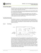
MT9P031: 1/2.5-Inch 5Mp Digital Image Sensor General Description General Description The MT9P031 sensor can be operated in its default mode or programmed by the user for frame size, exposure, gain setting, and other parameters. The default mode outputs a full resolution image at 14 frames per second (fps). An on-chip analog-to-digital converter (ADC) provides 12 bits per pixel. FRAME_VALID (FV) and LINE_VALID (LV) signals are output on dedicated pins, along with a pixel clock that is synchronous with valid data. The MT9P031produces extraordinarily clear, sharp digital pictures, and its ability...
Open the catalog to page 6
MT9P031: 1/2.5-Inch 5Mp Digital Image Sensor Functional OverviewFigure 2: Typical Configuration (Connection) -m—*- Saddr <■ RESET_BAR ■c STANDBY BAR Master clock SCLK Sdata TRIGGER Note: 1. A resistor value of 1.5kQ is recommended, but may be greater for slower two-wire speed. 2. All power supplies should be adequately decoupled. 3. All Dgnd pins must be tied together, as must all Agnd pins, all Vdd_IO pins, and all Vdd pins. Figure 3: 48-Pin iLCC 10 x 10 Package Pinout Diagram (Top View) frame_validiz line_validc STROBE Dgnd Vdd_IO|Z Vdd Saddr STANDBY_BAR|Z TRIGGER RESET_BAR|Z OE NC...
Open the catalog to page 7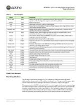
MT9P031: 1/2.5-Inch 5Mp Digital Image Sensor Pixel Data Format Table 3: Pin Description Pixel Data Format Pixel Array Structure The MT9P031 pixel array consists of a 2752-column by 2004-row matrix of pixels addressed by column and row. The address (column 0, row 0) represents the upper-right corner of the entire array, looking at the sensor, as shown in Figure 4 on page 9. The array consists of a 2592-column by 1944-row active region in the center representing the default output image, surrounded by a boundary region (also active), surrounded by a border of dark pixels (see Table 4 and Table...
Open the catalog to page 8All The Imaging Source Europe GmbH catalogs and technical brochures
 MT9T031
12 Pages
 MT9J003
77 Pages
 IMAGINGSOURCE- Catalog
172 Pages
 dfgsdg
2 Pages


- DC power supply
- Electrical cable
- Digital imager
- AC/DC power supply
- Visible imager
- CMOS camera module
- Industrial camera module
- Infrared imager
- Monitoring camera system
- Full-color camera system
- USB camera module
- Single-output power supply
- Electrical data cable
- Image processing camera module
- Monochrome camera module
- GigE Vision camera
- Compact imager
- Industrial cable
- Switch electrical cable