

- Products
- Catalogs
- News & Trends
- Exhibitions
iC-VRV 2x4 24 V Low-Side Driver with I/O Function and
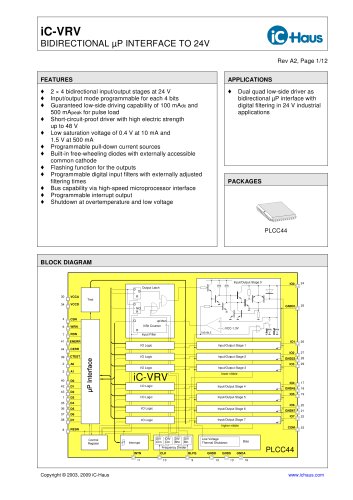
iC-VRV 2x4 24 V Low-Side Driver with I/O Function and
- 2x4 bidirectional input/output stages at 24V.
- Programmable input/output modes for each 4-bit group.
- Low-side driving capability of 100 mA continuous and 500 mA peak.
- Short-circuit protection and high electric strength up to 48V.
- Low saturation voltage and programmable pull-down current sources.
- Built-in free-wheeling diodes and flashing function for outputs.
- Programmable digital input filters and interrupt output.
- Shutdown features for overtemperature and low voltage.
- Supply Voltage: 4.5V to 5.5V.
- Operating Temperature: 0°C to 70°C.
- Thermal Resistance: 55 K/W.
- ESD Protection: 2 kV.
- Current and Voltage Ratings: Various limits for supply voltage, current in COM and IO pins, and peak currents.
- Chip programming via four addresses with control words for flashing frequencies, filtering times, interrupt control, and more.
- Interrupt generation can be activated for each I/O stage with input function.
- Test mode available for system testing via microprocessor interface.
Catalog excerpts
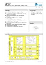
iC-VRV BIDIRECTIONAL ìP INTERFACE TO 24V Rev A2, Page 1/12 PLCC44 FEATURES APPLICATIONS Ë 2 × 4 bidirectional input/output stages at 24 V Ë Input/output mode programmable for each 4 bits Ë Guaranteed low-side driving capability of 100 mAdc and 500 mApeak for pulse load Ë Short-circuit-proof driver with high electric strength up to 48 V Ë Low saturation voltage of 0.4 V at 10 mA and 1.5 V at 500 mA Ë Programmable pull-down current sources Ë Built-in free-wheeling diodes with externally accessible common cathode Ë Flashing function for the outputs Ë Programmable digital input filters with externally adjusted filtering times Ë Bus capability via high-speed microprocessor interface Ë Programmable interrupt output Ë Shutdown at overtemperature and low voltage Ë Dual quad low-side driver as bidirectional ìP interface with digital filtering in 24 V industrial applications PACKAGES BLOCK DIAGRAM Copyright © 2003, 2009 iC-Haus www.ichaus.com iC-VRV Register Input/Output Stage 7 Input/Output Stage 6 Input/Output Stage 5 Input/Output Stage 4 Input/Output Stage 3 Input/Output Stage 2 Input/Output Stage 1 I/O Logic I/O Logic I/O Logic I/O Logic I/O Logic I/O Logic I/O Logic DISABLE higher nibble lower nibble Q Input/Output Stage 0 VCC-1.3V Thermal Shutdown Bias Low Voltage Frequency Divider Interrupt R Bln DIV Bhn DIV Cln DIV Chn DIV D D Q NQ R R Control Test Input Filter Output Latch up/dwn 3 Bit Counter CTEST ENERR CERR GNDD GNDS GNDA D0 D1 D2 D3 D5 D6 IO0 GND01 IO1 IO2 GND23 IO3 IO4 GND45 IO5 IO6 GND67 IO7 COM INTN CLK BLFQ RESN D7 D4 RDN WRN VCCD VCCA CSN A0 A1 34 30 6 4 41 7 44 39 2 3 40 42 43 1 35 36 37 38 8 11 10 9 12 13 16 24 25 26 27 28 23 22 21 20 19 18 17 29 PLCC44
Open the catalog to page 1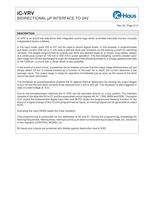
iC-VRV BIDIRECTIONAL ìP INTERFACE TO 24V Rev A2, Page 2/12 DESCRIPTION iC-VRV is an 8-fold low-side driver with integrated control logic which is divided internally into two mutually independent blocks (nibbles). In the input mode, ports IO0 to IO7 can be used to record logical levels. In this process, a programmable pull-down current (200 ìA or 2 mA) sets a defined level and functions as the biasing current for switching contacts. The stages programmed as outputs can drive any desired loads (e. g. lamps, long cables, relays) at a continuous current of 100 mA or 500 mA in pulse operation. The...
Open the catalog to page 2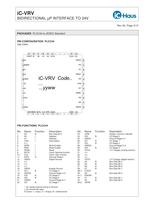
iC-VRV BIDIRECTIONAL ìP INTERFACE TO 24V Rev A2, Page 3/12 PACKAGES PLCC44 to JEDEC Standard PIN CONFIGURATION PLCC44 (top view) PIN FUNCTIONS PLCC44 No. Name Function Description No. Name Function Description 1 D3 B Bus Data Bit 3 23 COM Diodes, common cathode 2 A0 I Address 24 IO0 B I/O Stage 0 3 A1 I Address 25 GND01 Ground Stage 0+1 4 CSN I Chip Select 26 IO1 B I/O Stage 1 5 n.c. 27 IO2 B I/O Stage 2 6 WRN I Write Enable 28 GND23 Ground Stage 2+3 7 RDN I Read Enable 29 IO3 B I/O Stage 3 8 RESN I Reset 30 VCCA +5 V Supply (analog section) 9 BLFQ I Clock, flashing function 31 n.c. 10 CLK I...
Open the catalog to page 3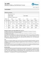
iC-VRV BIDIRECTIONAL ìP INTERFACE TO 24V Rev A2, Page 4/12 PROGRAMMING Selection of functions Data Word D7..D0 higher nibble lower nibble Selected I/O Stage function: Address Input Output Input Output A1 A0 Write Read Write Read Write Read Write Read 0 0 Test Pattern IR Inputs Outputs Outputs Test Pattern IR Inputs Outputs Outputs 0 1 IR Enable IR Enable Pulse Enable Pulse Enable IR Enable IR Enable Pulse Enable Pulse Enable 1 0 Control Word 2 Inputs Control Word 2 Feedback I/O Stages Control Word 2 Inputs Control Word 2 Feedback I/O Stages 1 1 Control Word 1 Control Word 1 Control Word 1 Control...
Open the catalog to page 4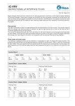
iC-VRV BIDIRECTIONAL ìP INTERFACE TO 24V Rev A2, Page 5/12 Signal changes which would be relevant for an interrupt generation could occur in the read-out phase following an interrupt message. These signal changes are lost when the interrupt register is deleted. As an alternative, the read-out of the interrupt register is possible (functional selection: read IR inputs). The registers can then be reset separately by blocking the IR enable for each reporting stage singly and then releasing it (functional selection: IR enable). Filter periods The input comparator of each I/O stage switches the counting...
Open the catalog to page 5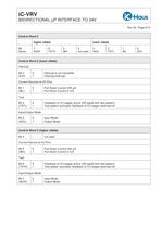
iC-VRV BIDIRECTIONAL ìP INTERFACE TO 24V Rev A2, Page 6/12 Control Word 2 higher nibble lower nibble Bit Name 7 NIOH 6 TSTH 5 IBH 4n ot used 3 NIOL 2 TSTL 1 IBL 0 EOI Control Word 2 (lower nibble) Interrupt Bit 0 (EOI) 01 Interrupt is not cancelled Clearing Interrupt Current Sources at I/O Pins Bit 1 (IBL) 01 Pull-Down Current 200 ìA Pull-Down Current 2 mA Test Bit 2 (TSTL) 01 Feedback of I/O stages active (OR gated with test pattern) Test pattern activated, feedback of I/O stages switched off Input/Output Mode Bit 3 (NIOL) 01 Input Mode Output Mode Control Word 2 (higher nibble) Bit 4 - not...
Open the catalog to page 6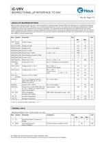
iC-VRV BIDIRECTIONAL ìP INTERFACE TO 24V Rev A2, Page 7/12 All voltages are referenced to ground unless otherwise noted. All currents into the device pins are positive; all currents out of the device pins are negative. ABSOLUTE MAXIMUM RATINGS Beyond these values damage may occur; device operation is not guaranteed. Absolute Maximum Ratings are no Operating Conditions. Integrated circuits with system interfaces, e.g. via cable accessible pins (I/O pins, line drivers) are per principle endangered by injected interferences, which may compromise the function or durability. The robustness of the...
Open the catalog to page 7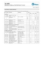
iC-VRV BIDIRECTIONAL ìP INTERFACE TO 24V Rev A2, Page 8/12 ELECTRICAL CHARACTERISTICS Operating Conditions: VCC= VCCA= VCCD= 5V ±10%, Tj= 0..125°C, unless otherwise noted Item Symbol Parameter Conditions Tj Fig. Unit °C Min. Typ. Max. Total Device 001 VCCA VCCD Permissible Supply Voltage Range 4.5 5.5 V 002 I(VCCA) Supply Current in VCCA, power section IO0..7= lo, unloaded 0 27 70 125 5555 65 60 55 55 mA mA mA mA 003 I(VCCD) Supply Current in VCCD, digital section all logic inputs lo= 0V or hi= VCC 0 10 mA 004 I(VCCD) Supply Current in VCCD, digital section all logic inputs lo= 0.8V 80 mA 005...
Open the catalog to page 8All IC-Haus catalogs and technical brochures
 Product Line Card
6 Pages
 iC-TL46 BLCC SD1C Blue LED
7 Pages
 iC212 HIGHSPEED PHOTORECEIVER
16 Pages
 Product overview
6 Pages






Archived catalogs
 iC-OV 5-Bit Optical Encoder
9 Pages
 Laser Webinar Handout
14 Pages
- Angular encoder
- Proximity switch
- Absolute rotary encoder
- Position transducer
- Photoelectric sensor
- Multipole switch
- Optical rotary encoder
- Transceiver module
- Linear position transmitter
- Magnetic rotary encoder
- Rectangular photoelectric sensor
- Flow sensor
- Linear encoder
- Volume flow sensor
- Signal conditioner
- Touch switch
- Magnetic position sensor
- Infrared photoelectric sensor
- Magnetic proximity sensor
- Metal position sensor