iC-MFL, iC-MFLT 8-/12-Fold Fail-Safe Logic N-FET Driver
1 /13Pages

iC-MFL, iC-MFLT 8-/12-Fold Fail-Safe Logic N-FET Driver
1 /13Pages
Catalog excerpts
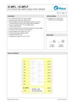
iC-MFL / iC-MFLT 8-/12-FOLD FAIL-SAFE LOGIC N-FET DRIVER Rev C1, Page 1/13 FEATURES o 8-/12-fold level shift to 5 V output voltage o Safe low output state with single errors o Schmitt trigger inputs with two-stage pull-down current for enhanced noise immunity with limited power dissipation o Inputs compatible with TTL and CMOS levels (1.8 V to 3.3 V to 5 V) o Current-limited and short-circuit-proof push-pull output stages o Push-pull current sources for driving FETs o Surge voltage-proof outputs up to 18 V o Ground and supply voltage monitor o Protective ESD circuitry o Temperature range from -40 to 125 °C o Operation of 5 V logic level N-FETs from 3.3 V systems BLOCK DIAGRAM Supply- and Ground Monitor
Open the catalog to page 1
iC-MFL / iC-MFLT 8-/12-FOLD FAIL-SAFE LOGIC N-FET DRIVER Rev C1, Page 2/13 DESCRIPTION iC-MFL / iC-MFLT is a monolithically integrated, 8/12-channel level adjustment device which drives N-channel FETs. The internal circuit blocks have been designed in such a way that with single errors, such as open pins (VCC, GND, GNDR) or the short-circuiting of two outputs, iC-MFL’s output stages switch to a predened, safe low state. Externally connected N-channel FET are thus shut down safely in the event of a single error. The inputs of the eight/twelve channels consist of a Schmitt trigger with a pull-down...
Open the catalog to page 2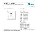
iC-MFL / iC-MFLT 8-/12-FOLD FAIL-SAFE LOGIC N-FET DRIVER Rev C1, Page 3/13 PIN CONFIGURATION QFN24 4 mm x 4 mm to JEDEC MO220 5 V Output channel 1 (n.c.) (n.c.) Ground (Resistor) 5 V Supply Voltage Input channel 1 Input channel 2 Input channel 3 Input channel 4 Input channel 5 Input channel 6 Input channel 7 Input channel 8 (n.c.) Enable Input (n.c.) Ground 5 V Output channel 8 5 V Output channel 7 5 V Output channel 6 5 V Output channel 5 5 V Output channel 4 5 V Output channel 3 5 V Output channel 2 Thermal-Pad The Thermal Pad is to be connected to a ground plane on the PCB. Connections between...
Open the catalog to page 3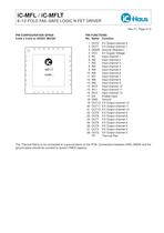
iC-MFL / iC-MFLT 8-/12-FOLD FAIL-SAFE LOGIC N-FET DRIVER Rev C1, Page 4/13 PIN FUNCTIONS No. Name Function 5 V Output channel 2 5 V Output channel 1 Ground (Resistor) 5 V Supply Voltage Input channel 1 Input channel 2 Input channel 3 Input channel 4 Input channel 5 Input channel 6 Input channel 7 Input channel 8 Input channel 9 Input channel 10 Input channel 11 Input channel 12 Enable Input Ground 5 V Output channel 12 5 V Output channel 11 5 V Output channel 10 5 V Output channel 9 5 V Output channel 8 5 V Output channel 7 5 V Output channel 6 5 V Output channel 5 5 V Output channel 4 5 V Output...
Open the catalog to page 4
iC-MFL / iC-MFLT 8-/12-FOLD FAIL-SAFE LOGIC N-FET DRIVER Rev C1, Page 5/13 ABSOLUTE MAXIMUM RATINGS Beyond these values damage may occur; device operation is not guaranteed. Item No. Supply Voltage Voltage at GNDR referenced to GND Voltage at GND referenced to GNDR Operating Junction Temperature Storage Temperature Range THERMAL DATA Operating Conditions: VCC = 5 V ±10 % Item No. Operating Ambient Temperature Range Thermal Resistance Chip/Ambient -40 SMD assembly, no additional cooling areas. All voltages are referenced to ground unless otherwise stated. All currents into the device pins are...
Open the catalog to page 5
iC-MFL / iC-MFLT 8-/12-FOLD FAIL-SAFE LOGIC N-FET DRIVER Rev C1, Page 6/13 ELECTRICAL CHARACTERISTICS Operating Conditions: VCC = 5 V ±10 %, Tj = -40...125 °C unless otherwise stated Item No. Permissible Supply Voltage (No load) iC-MFL iC-MFLT (No load) iC-MFL iC-MFLT (No load, all OUTx = hi) iC-MFL iC-MFLT Current Driver OUT1...8/12 101 I(OUTx) Current in I(OUTx) permitted voltage Clamp Voltage lo referenced to I() = -10 mA the lower voltage of GND, GNDR Saturation Voltage hi referenced to VCC Saturation Voltage lo referenced to GND Pull-Down Resistor at OUTx referenced to GNDR Short circuit...
Open the catalog to page 6
iC-MFL / iC-MFLT 8-/12-FOLD FAIL-SAFE LOGIC N-FET DRIVER Rev C1, Page 7/13 ELECTRICAL CHARACTERISTICS Operating Conditions: VCC = 5 V ±10 %, Tj = -40...125 °C unless otherwise stated Item No. 406 Symbol Vtr()hys ({INx, EN}lo → hi) → 90 % OUTx, ({INx, EN}hi → lo) → 10 % OUTx, no Cl() Vt()hys = Vt()hi - Vt()lo Propagation Delay, INx, EN → OUTx
Open the catalog to page 7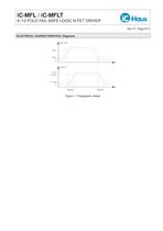
iC-MFL / iC-MFLT 8-/12-FOLD FAIL-SAFE LOGIC N-FET DRIVER Rev C1, Page 8/13 ELECTRICAL CHARACTERISTICS: Diagrams V(INx, EN) Figure 1: Propagation delays
Open the catalog to page 8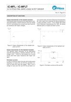
iC-MFL / iC-MFLT 8-/12-FOLD FAIL-SAFE LOGIC N-FET DRIVER Rev C1, Page 9/13 DESCRIPTION OF FUNCTIONS Output characteristic of the lowside transistor The lowside output transistors at the eight/twelve channels demonstrate a resistive behavior with low voltage V(OUTx) and behave as a current sink with nite output resistance with higher voltages. I(OUTx) rent remains high until Vt()hi (Electrical Characteristics No. 203); above this threshold the device switches to a lower pull-down current. If the voltage falls below Vt()lo (Electrical Characteristics No. 204), the device switches back to a higher...
Open the catalog to page 9
iC-MFL / iC-MFLT 8-/12-FOLD FAIL-SAFE LOGIC N-FET DRIVER Rev C1, Page 10/13 DETECTING SINGLE ERRORS If single errors are detected, safety-relevant applications require externally connected switching transistors to be specically shut down. Single errors can occur when a pin is open (due to a disconnected bonding wire or a bad solder connection, for example) or when two pins are short-circuited. When two output of different logic levels are shortcircuited, the driving capability of the lowside driver will predominate, keeping the connected N-channel FETs in a safe shutdown state. With open pins...
Open the catalog to page 10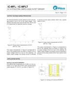
iC-MFL / iC-MFLT 8-/12-FOLD FAIL-SAFE LOGIC N-FET DRIVER Rev C1, Page 11/13 OUTPUT VOLTAGE SURGE PROTECTION An internal protective circuitry allows for short overvoltage pulses of up to 18 V at the output stages. Puls duration and duty cycle must be less than 100 ms and 2 % respectively for absolute maximum ratings. to ground via the output resistor which has a typical value of 150 Ω. I(OUTx) [mA] 80 Figure 8: Surge output characteristic at OUTx with Vin = low The output characteristic in Figure 8 corresponds to that of the lowside driver as shown in Figure 2 for an output voltage V(OUTx) of...
Open the catalog to page 11All IC-Haus catalogs and technical brochures
 Product Line Card
6 Pages
 iC-TL46 BLCC SD1C Blue LED
7 Pages
 iC212 HIGHSPEED PHOTORECEIVER
16 Pages
 Product overview
6 Pages


Archived catalogs
 iC-OV 5-Bit Optical Encoder
9 Pages
 Laser Webinar Handout
14 Pages
- ERLO rotary encoder
- Proximity switch
- ERLO absolute rotary encoder
- ERLO position sensor
- Multipole switch
- Transceiver module
- ERLO optical rotary encoder
- Photoelectric sensor
- ERLO linear position sensor
- ERLO magnetic rotary encoder
- Rectangular photoelectric sensor
- Flow sensor
- Linear encoder
- Touch switch
- Volume flow sensor
- ERLO signal conditioner
- ERLO magnetic position sensor
- Magnetic proximity sensor
- ERLO metal position sensor
- Remote control receiver