485165
1 /9Pages
485165
1 /9Pages
Catalog excerpts

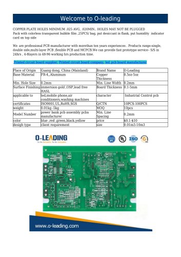
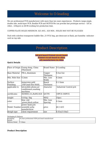
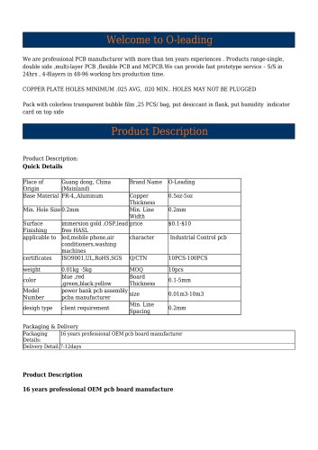
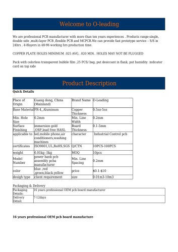
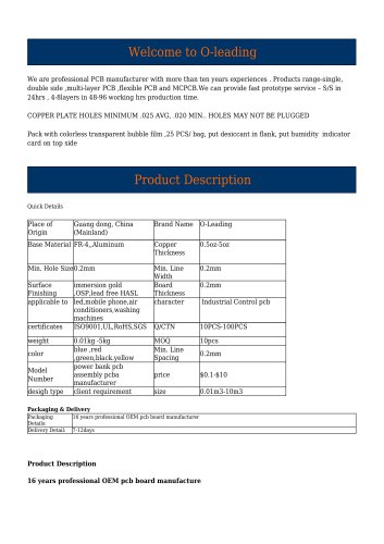
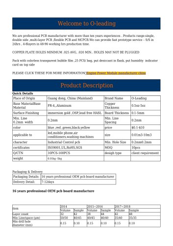
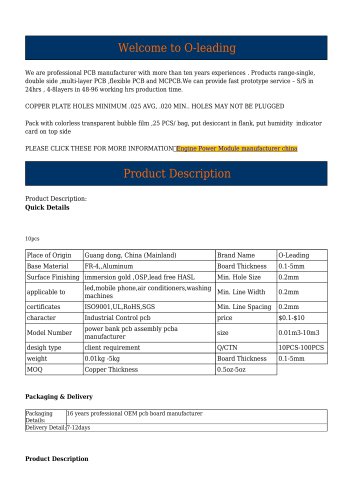
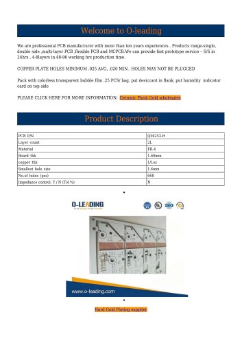
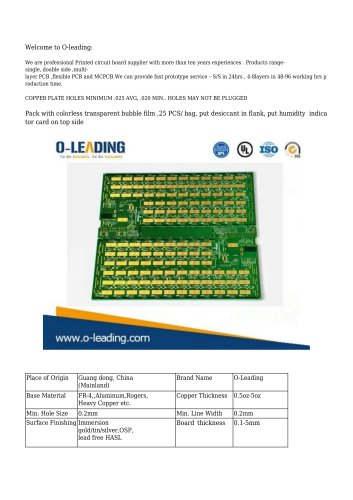
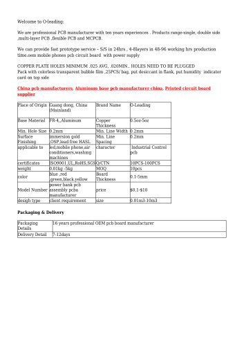
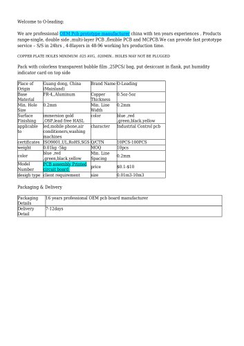
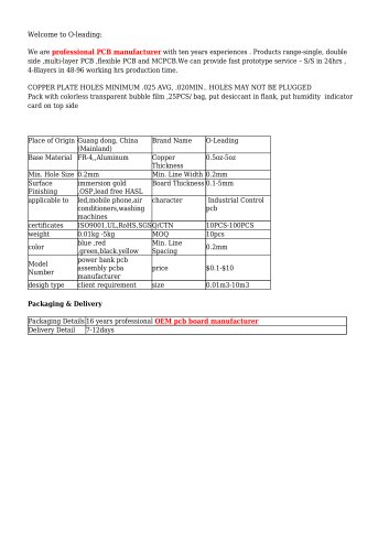
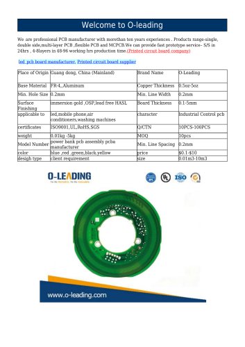
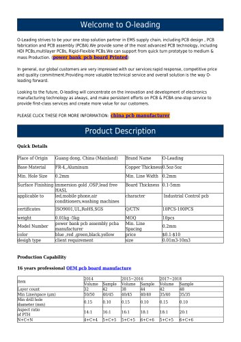
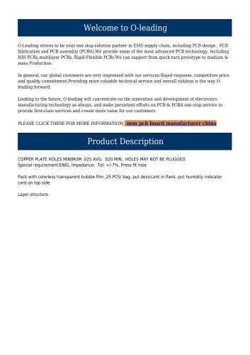
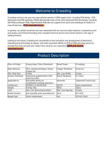
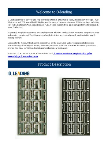
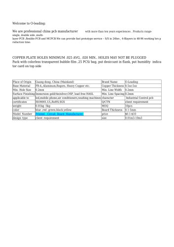
COPPER PLATE HOLES MINIMUM .025 AVG, .020MIN.. HOLES MAY NOT BE PLUGGED Pack with colorless transparent bubble film ,25PCS/ bag, put desiccant in flank, put humidity indicator We are professional PCB manufacturer with morethan ten years experiences . Products range-single, double side,multi-layer PCB ,flexible PCB and MCPCB.We can provide fast prototype service- S/S in 24hrs , 4-8layers in 48-96 working hrs production time. Printed circuit board supplier, Printed circuit board company, led pcb board manufacturer
Open the catalog to page 1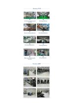
High-speed flying probe E-test Machine
Open the catalog to page 3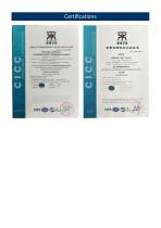
CertificationsQUALITY MANAGEMENT SYSTEM CERTIFICATE We hereby certify that QkM No alaai^ldcoJi'iH Art fl>TRV im »7* TAJ SANG BANK BUBIfelG 1J0-1X2 DCS VOf US BCAO CSNTRAl HK Bw»a»m AM 1311 T'OO' 13. roV« OXV'fJ twi Hyya'-J CNfict KAtficw OubVJong C*na Mm »rnpt*mo«*ad and maintom a Quality Managamant Syatam Which Mia tha raquramanU of tha kxkwng atandanJa GarT1B001-20tB *X IS09001 2015 Scopo of certification Sale* of pnrXad orcurt board* tnaal luoance panod ratyjary 77. 201* Tha carVcafa a r j*d ft/wj Apr* 32. 7019 FatKuary 20. 7021 Tha oanflcata a rvM a INoU CCC Qua*#* hbal m fa kacwwnq panod
Open the catalog to page 4
SGS Test Report No.SZXEC1900530401 Date: 30 Mar 2019 Page lot 6 O-LEADING SUPPLY CHAIN (HK) CO,LIMITED 1313.FLOOR 13. FORTUNE BUILDING, DANSHUI TOWN. HUIYANG DISTRICT. HUIZHOU. GUANGDONG. CHINA The following sample(s) was/were submitted and identified on behalf of the clients as Date of Sample Received : Testing Period : Test Requested : Test Method : 22 Mar 2319 - 30 Mar 2019 Selected test(s) as requested by client Please refer to next page(s). Test Report Test Results: Test Part Description Specimen No. SGS Sample ID Description (2) MDL = Method Detection Limit Test Results : Please refer to...
Open the catalog to page 5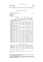
WIRING, PRINTED - COMPONENT | UL Product iQ See General Information for Wiring, Printed Component O-LEADING SUPPLY CHAIN (HK) CO LTD E490354 ROOM 1205, 12/F TAI SANG BANK BLDG CENTRAL, HONG KONG Solder Oper Meets C Limits Temp Flame UL796 T C sec C Class DSR I mm(in) mic(mil) DSO mm(in) * - CTI marking is optional and may be marked on the printed wiring board. Marking: Company name or file number and type designation. May be followed by a suffix to denote factory identification or burning test classification. uLLAiiE, #iit£uL atMPSLtrostu
Open the catalog to page 6
Packaging & Delivery
Open the catalog to page 7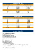
Process Capability PCB Production Capabilities Layer Count: 1Layer-32Layer Finished copper thickness: 1/3oz-12oz Min Line width/spacing internal: 3.0mil/3.0mil Min Line width/spacing external: 4.0mil/4.0mil Max Aspect Ratio: 10:1 Board thickness: 0.2mm-5.0mm Max Panel size(inches): 635*1500mm Minimum Drilled Hole Size: 4mil PIated Hole Tolerance: +/-3mil BIind/Buried Vias (AII Types): YES Via Fill(Conductive,Non-Conductive): YES Base Material: FR-4,FR-4high Tg.Halogen free material,Rogers,Aluminium base,Polyimide, Heavy Copper Surface finishes: HASL,OSP,ENIG,HAL-LF,lmmersion silver,lmmersion Tin,Gold...
Open the catalog to page 8
PCB Material: FR-4,CEM-1,CEM-3,Aluminum-based board Max PCB size: 510x460mm Min PCB size:50x50mm PCB Thickness:0.5mm-4.5mm Board thickness:0.5-4mm Min Components size: 0201 Standard chip size component: 0603 and larger Component max height:15mm Min lead pitch: 0.3mm Min BGA ball pitch:0.4mm Placement precision: +/-0
Open the catalog to page 9All HUIZHOU OLEADING TECHNOLOGY CO., LIMITED catalogs and technical brochures
 117_D53
8 Pages
 076-52
8 Pages
 128-GH
8 Pages
 1CP_R5
8 Pages
 86-423
8 Pages
 12421-GPOU
8 Pages
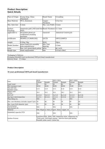
 Q56253-H
6 Pages
 28754
287542 Pages
 2857
28574 Pages
 2512748
2 Pages
 25117577
2 Pages
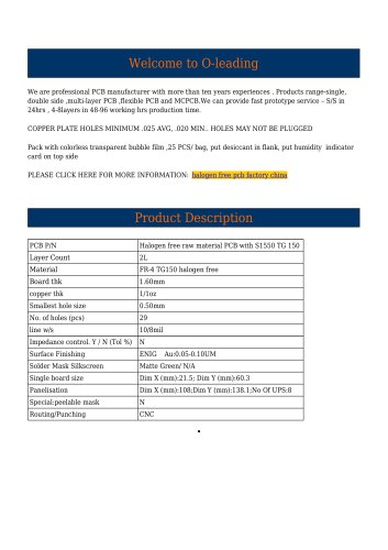 S1550 TG 150
8 Pages
 842378
2 Pages
 84312
843122 Pages
 3837865
9 Pages
 104_DCP_R2
3 Pages
 Power bank pcb board Printed)
13 Pages
 PCB
PCB11 Pages
 HI series
10 Pages
 2231I0009
19 Pages
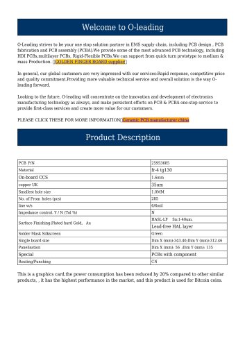 25953685
10 Pages
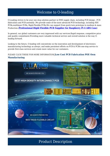 Raspberry Pi 4
20 Pages
 Raspberry Pi 3 Model A+
20 Pages
 2876414
2 Pages
- Digital I/O
- IO module
- Digital IO module
- Single-board computer
- Communication module
- Ethernet IO module
- HDMI single-board computer
- USB single-board computer
- Ethernet communication module
- USB I/O
- ARM architecture single-board computer
- PCBA for industrial applications
- WiFi single-board computer
- Custom-made PCB
- Electronic PCBA
- USB I/O module
- Standard I O module
- Multilayer PCBA
- Pico-ITX single-board computer