25953685
1 /10Pages

25953685
1 /10Pages
Catalog excerpts
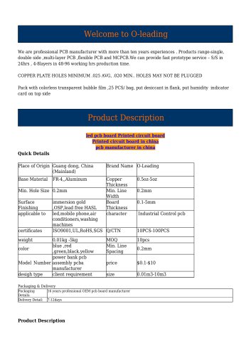
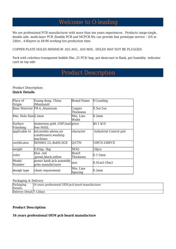
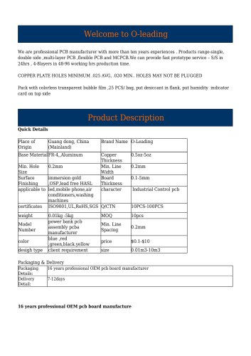
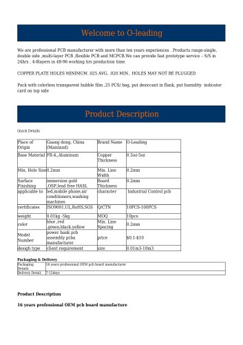
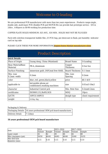
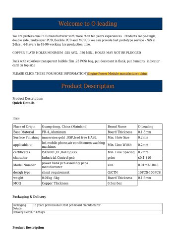
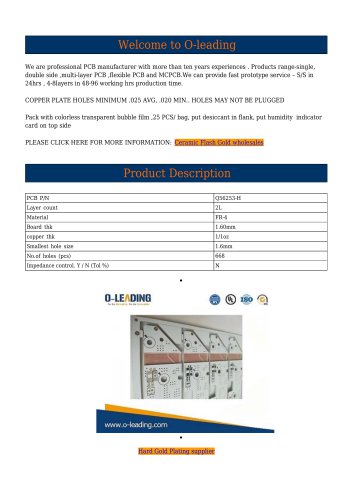
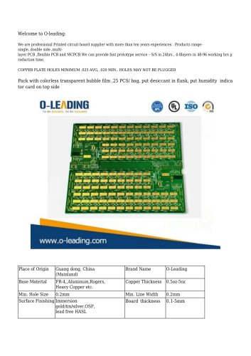
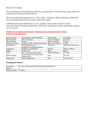
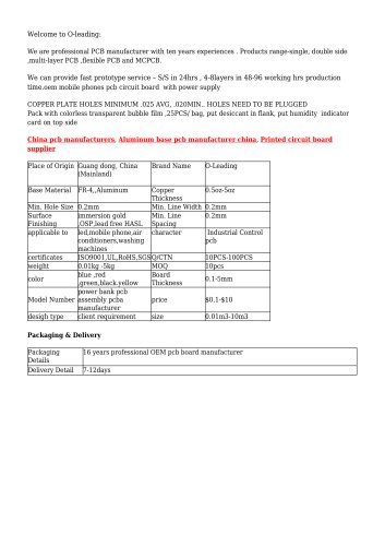
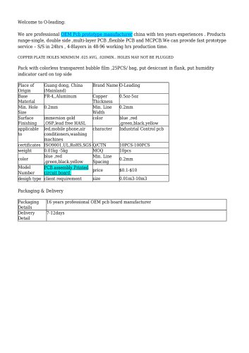
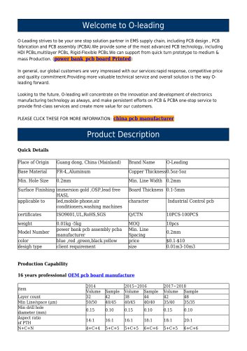
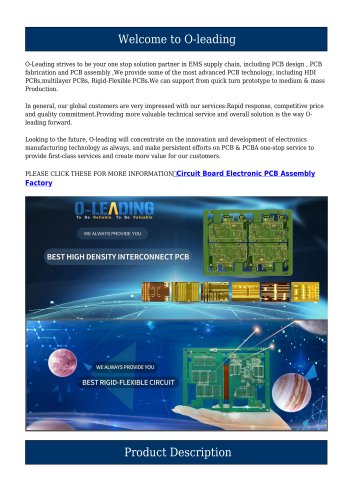
Welcome to O-leading O-Leading strives to be your one stop solution partner in EMS supply chain, including PCB design , PCB fabrication and PCB assembly (PCBA).We provide some of the most advanced PCB technology, including HDI PCBs,multilayer PCBs, Rigid-Flexible PCBs.We can support from quick turn prototype to medium & mass Production. (GOLDEN FINGER BOARD supplier) In general, our global customers are very impressed with our services:Rapid response, competitive price and quality commitment.Providing more valuable technical service and overall solution is the way Oleading forward. Looking to the future, O-leading will concentrate on the innovation and development of electronics manufacturing technology as always, and make persistent efforts on PCB & PCBA one-stop service to provide first-class services and create more value for our customers. PLEASE CLICK THESE FOR MORE INFORMATION:Ceramic PCB manufacturer china Smallest hole size Surface Finishing:Plated hard Gold, Au Solder Mask Silkscreen Single board size PCBs with component This is a graphics card,the power consumption has been reduced by 20% compared to other similar products, , it has the highest performance in the market, and this product is used for Bitcoin coi
Open the catalog to page 1
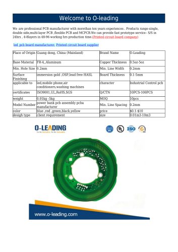
LED PCB board, circuit board
Open the catalog to page 2
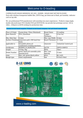
Packaging & Delivery
Open the catalog to page 8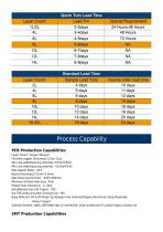
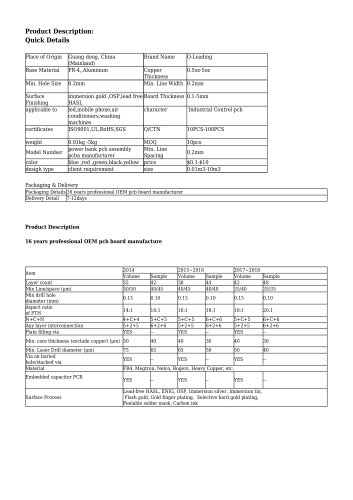
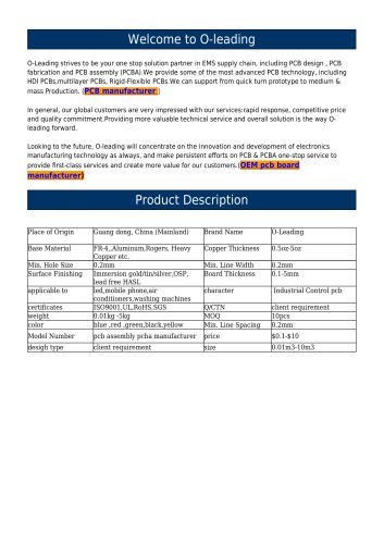
Process Capability PCB Production Capabilities Layer Count: 1Layer-32Layer Finished copper thickness: 1/3oz-12oz Min Line width/spacing internal: 3.0mil/3.0mil Min Line width/spacing external: 4.0mil/4.0mil Max Aspect Ratio: 10:1 Board thickness: 0.2mm-5.0mm Max Panel size(inches): 635*1500mm Minimum Drilled Hole Size: 4mil PIated Hole Tolerance: +/-3mil BIind/Buried Vias (AII Types): YES Via Fill(Conductive,Non-Conductive): YES Base Material: FR-4,FR-4high Tg.Halogen free material,Rogers,Aluminium base,Polyimide, Heavy Copper Surface finishes: HASL,OSP,ENIG,HAL-LF,lmmersion silver,lmmersion Tin,Gold...
Open the catalog to page 9
PCB Material: FR-4,CEM-1,CEM-3,Aluminum-based board Max PCB size: 510x460mm Min PCB size:50x50mm PCB Thickness:0.5mm-4.5mm Board thickness:0.5-4mm Min Components size: 0201 Standard chip size component: 0603 and larger Component max height:15mm Min lead pitch: 0.3mm Min BGA ball pitch:0.4mm Placement precision: +/-0
Open the catalog to page 10All HUIZHOU OLEADING TECHNOLOGY CO., LIMITED catalogs and technical brochures
 117_D53
8 Pages
 076-52
8 Pages
 128-GH
8 Pages
 1CP_R5
8 Pages
 86-423
8 Pages
 12421-GPOU
8 Pages
 Q56253-H
6 Pages
 28754
287542 Pages
 2857
28574 Pages
 2512748
2 Pages
 25117577
2 Pages
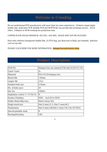 S1550 TG 150
8 Pages
 842378
2 Pages
 84312
843122 Pages
 3837865
9 Pages
 485165
9 Pages
 104_DCP_R2
3 Pages
 Power bank pcb board Printed)
13 Pages
 PCB
PCB11 Pages
 HI series
10 Pages
 2231I0009
19 Pages
 Raspberry Pi 4
20 Pages
 Raspberry Pi 3 Model A+
20 Pages
 2876414
2 Pages
- Digital I/O
- IO module
- Digital IO module
- Single-board computer
- Communication module
- PCB
- Ethernet IO module
- HDMI single-board computer
- USB single-board computer
- Ethernet communication module
- USB I/O
- ARM architecture single-board computer
- PCBA for industrial applications
- WiFi single-board computer
- Custom-made PCB
- Electronic PCBA
- USB I/O module
- Standard I O module
- Multilayer PCBA
- Pico-ITX single-board computer