076-52
1 /8Pages
076-52
1 /8Pages
Catalog excerpts
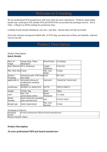
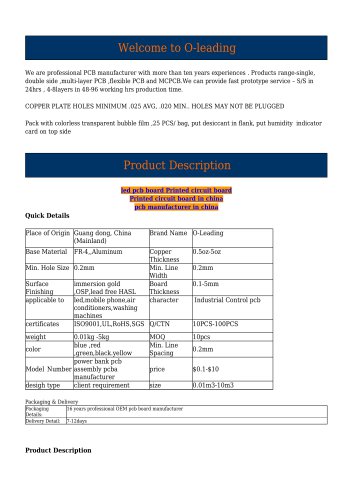
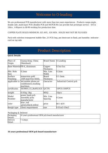
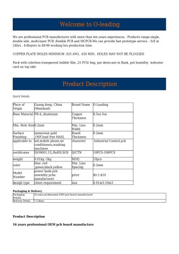
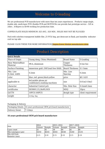
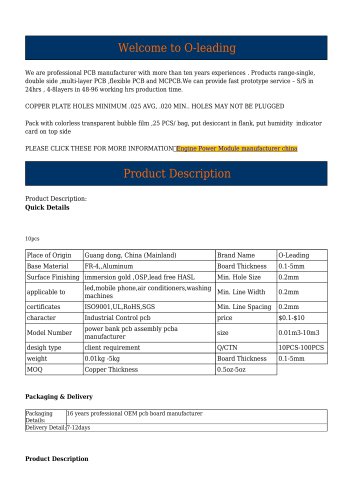
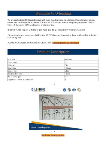
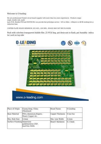
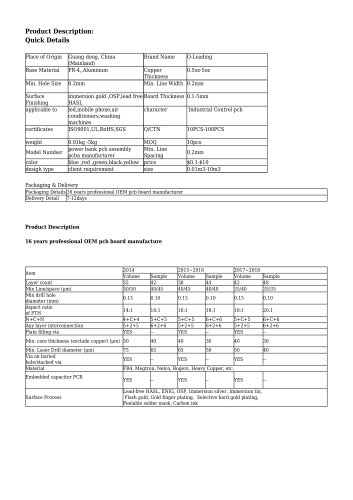
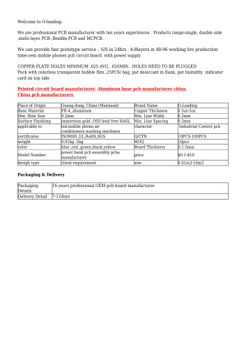
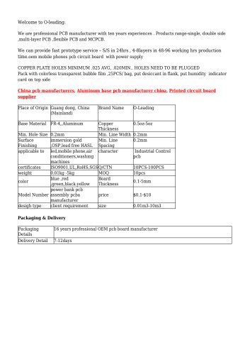
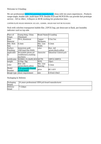
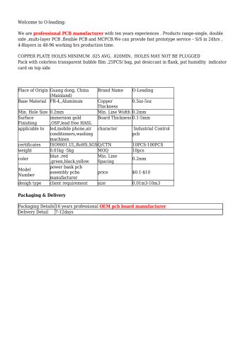
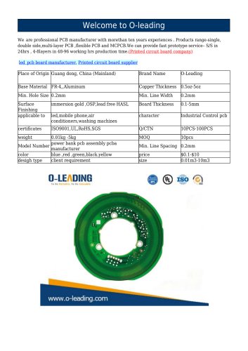
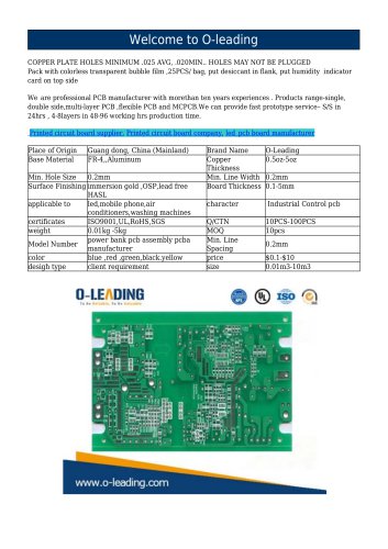
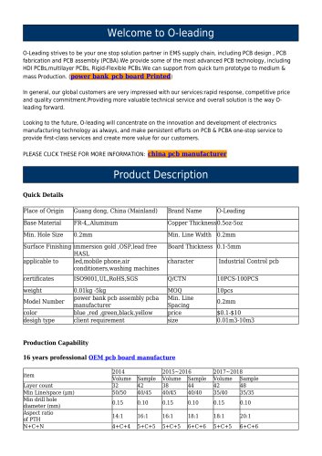
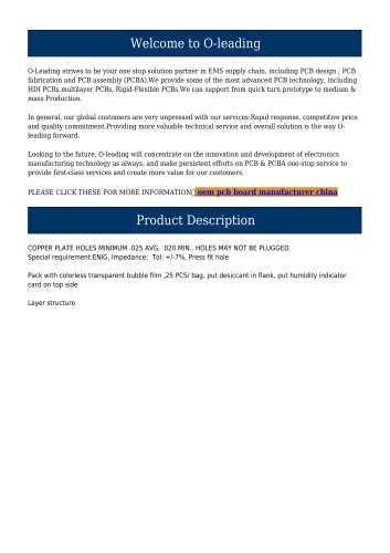
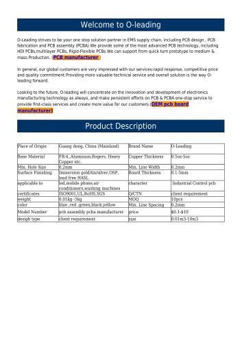
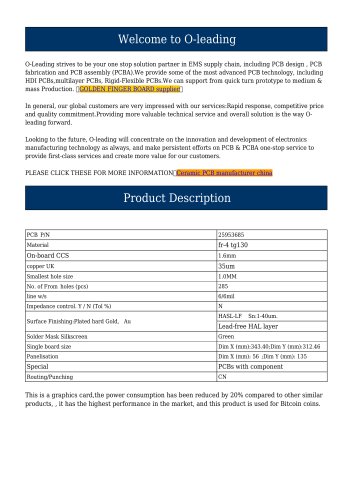
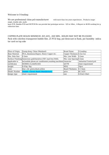
We are professional PCB manufacturer with more than ten years experiences . Products range-single, double side ,multi-layer PCB ,flexible PCB and MCPCB.We can provide fast prototype service - S/S in 24hrs , 4-8layers in 48-96 working hrs production time. COPPER PLATE HOLES MINIMUM .025 AVG, .020 MIN.. HOLES MAY NOT BE PLUGGED Pack with colorless transparent bubble film ,25 PCS/ bag, put desiccant in flank, put humidity indicator card on top side Product Description: Quick Details
Open the catalog to page 1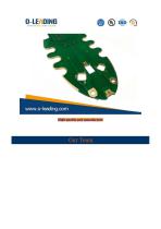
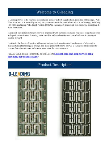
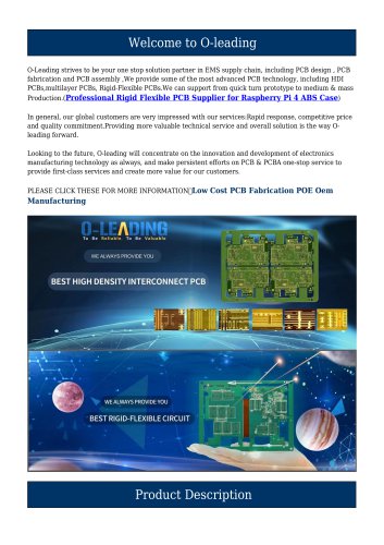
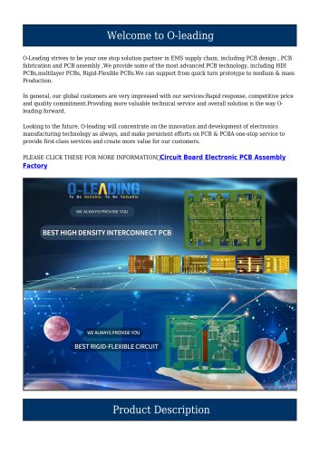
High quality pcb manufacture
Open the catalog to page 3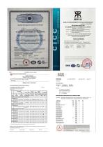
Quality Management System Certificate fOrp—oeu—»codt cn«iiim« uMisfi-oog-ar it-ei •Ota l/« NAM6 PONT COMMIICMl IUUOMG. It' CMlUNO CM A WAN. «l *>« tftebillhed the que lily menegement Iflitfl requirement! of ftenderd Certlflietlon «ddre*t; Scorn 111» fortune BudiHn* Nenhtng Weft Hoed. Muiy.ng Dtftrnt. Mulehou. Gue ngdong. Chine C.r tlf Met Ion AdMtN* Site* end •erviidf 0• printed duett boerdi Intttei timed Dm ffllHllt »i emit Pete — WVr-j, Printed - Component rr'unrm*ir<te<»*,. ;!••••-.M* I Clrt -r • prr.rt: rr Pr'.n'*H-n nr .-rnrIrfviwtiiv Wiring, Printed - Component Q-CCABIHC itmt CHAIN CO UWIEO...
Open the catalog to page 6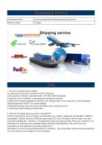
1. How do O-Leading ensure quality? Our high quality standard is achieved with the following. 1. The process is strictly controlled under ISO 9001:2008 standards. 2. Extensive use of software in managing the production process 3.State-of-art testing equipments and tools. E.g. Flying Probe, X-ray Inspection, AOI (Automated Optical Inspector) and ICT (in-circuit testing). 4. Dedicated quality assurance team with failure case analysis process 5. Continuous staff training and education 2. How do O-Leading keep your price competitive? Over the last decade, prices of many raw materials (e.g. copper,...
Open the catalog to page 7
3. What kinds of boards can O-Leading process? Common FR4, high-TG and halogen-free boards, Rogers, Arlon, Telfon, aluminum/copper-based boards, PI, etc. 4. What data are needed for PCB production? It is best to provide data in Gerber 274-X format. In addition, Cam350, CAD, Protel 99se, PADS, DXP and Eagle can also be processed. 5. What’s the typical process flow for multi-layer PCB? Material cutting → Inner dry film → inner etching → Inner AOI → Multi-bond → Layer stack up Pressing → Drilling → PTH → Panel Plating → Outer Dry Film → Pattern Plating → Outer etching → Outer AOI → Solder Mask →...
Open the catalog to page 8All HUIZHOU OLEADING TECHNOLOGY CO., LIMITED catalogs and technical brochures
 117_D53
8 Pages
 128-GH
8 Pages
 1CP_R5
8 Pages
 86-423
8 Pages
 12421-GPOU
8 Pages
 Q56253-H
6 Pages
 28754
287542 Pages
 2857
28574 Pages
 2512748
2 Pages
 25117577
2 Pages
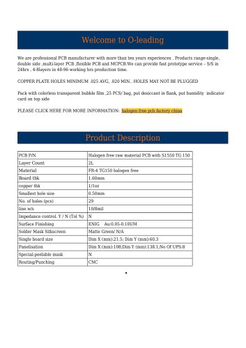 S1550 TG 150
8 Pages
 842378
2 Pages
 84312
843122 Pages
 3837865
9 Pages
 485165
9 Pages
 104_DCP_R2
3 Pages
 Power bank pcb board Printed)
13 Pages
 PCB
PCB11 Pages
 HI series
10 Pages
 2231I0009
19 Pages
 25953685
10 Pages
 Raspberry Pi 4
20 Pages
 Raspberry Pi 3 Model A+
20 Pages
 2876414
2 Pages
- Digital I/O
- IO module
- Digital IO module
- Single-board computer
- Communication module
- PCB
- Ethernet IO module
- HDMI single-board computer
- USB single-board computer
- Ethernet communication module
- USB I/O
- ARM architecture single-board computer
- PCBA for industrial applications
- WiFi single-board computer
- Custom-made PCB
- Electronic PCBA
- USB I/O module
- Standard I O module
- Multilayer PCBA
- Pico-ITX single-board computer