
- Catalogs
- Hitachi High-Tech Europe GmbH
- SU3900SE/SE Plus SU3800SE/SE Plus | High resolution Schottky SEM


- Company
- Products
- Catalogs
- News & Trends
- Exhibitions
SU3900SE/SE Plus SU3800SE/SE Plus | High resolution Schottky SEM
SU3900SE/SE Plus SU3800SE/SE Plus | High resolution Schottky SEM
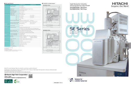
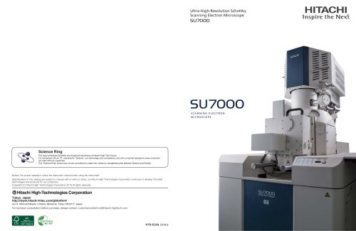
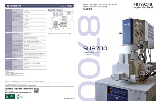
The SU3900SE/SE Plus and SU3800SE/SE Plus are high-resolution Schottky Scanning Electron Microscopes (SEMs) designed for large specimens with variable pressure functionality. Key specifications include a resolution of 0.9 nm at 30 kV, 2.5 nm at 1 kV, and 1.6 nm at 1 kV for SE Plus. The magnification range is from 5× to 600,000×. They feature a ZrO/W Schottky Emitter electron gun with an accelerating voltage from 0.5 kV to 30 kV. The stage control is a 5-axis motor drive, accommodating specimens up to 300 mm in diameter and 130 mm in height for the SU3900SE/SE Plus. Detectors include a Secondary Electron Detector (SED), TOP detector (TD), and optional detectors like an Energy Dispersive X-ray Spectrometer (EDS).
The SEMs require specific installation conditions: a temperature range of 15 to 25°C and humidity of 60% RH or less. The power supply needed is AC100-115 V, 2 kVA with D-type single grounding. A vacuum pump and air compressor are necessary for operation.
The SEMs offer high-resolution imaging for top-surface analysis with advanced Schottky optics. They include automation features like guided specimen exchange and auto alignment for improved usability. The variable pressure mode allows for non-conductive specimen observation, reducing charge artifacts.
These SEMs include features to enhance usability and efficiency, such as the EM Flow Creator for workflow automation, allowing for sequential image capture and parameter setting. User permission settings are available to customize access and prevent incorrect operation.
The SEMs are suitable for various applications, including automatic wide-area observation of semiconductor devices, detection of foreign matter during manufacturing using EDS particle analysis, and support for large specimens and specific location observation for quality management.
Specifications: The document provides a detailed analysis of various particles and alloys, including titanium oxide, Fe alloys, Cu alloys, and non-ferrous alloys. It categorizes particles based on their size and composition, focusing on Fe-Cr-Ni, Fe-Cu, high Fe, Cu-Fe, Cu, Al, Ni-Cu, Zn, Ti, and V.
Procedures: Particle size distribution is measured across different length scales, ranging from less than 5 µm to over 3000 µm, with data on the number of particles observed in each size category.
Applications: Applications include lithium-ion battery components, such as cathode materials and separators, where the distribution of particles and binders is analyzed. The document also covers the structure of carbon nanotubes and fuel-cell catalyst particles, highlighting the visibility of platinum particles.
Inorganic Materials: Analysis includes tungsten disulfide, iron, zinc oxide, high-entropy carbide films, and gallium nitride substrates, describing morphology and distribution, noting features like fine particle shapes and threading dislocations.
Key Observations: Titanium oxide particles are visible. Cathode material distributions in lithium-ion batteries are confirmed over wide areas. Carbon nanotubes exhibit interwoven structures with widths around 10 nm. Platinum particles in fuel-cell catalysts are visible with high contrast. Tungsten disulfide particles appear as stacked plate-like structures. Zinc oxide particles are approximately 50 nm in size. Gallium nitride substrates show threading dislocations using CL signal.
Conclusion: The document provides comprehensive data on particle size distribution and material composition, relevant for applications in battery technology and other fields involving inorganic materials.
Catalog excerpts

■ Installation example diagram Secondary Electron Image resolution High Resolution Schottky Scanning Electron Microscope ZrO/W Schottky Emitter Accelerating Voltage Stage Control Power cable Power cable Monitor Operation table φ130 mm φ 203 mm ( in combination with R ) φ 229 mm (*2) (in combination with R ) (in combination with R) Maximum Observable Height 130 mm (WD=10 mm) Max. φ 300 mm Mountable Specimen Size Maximum Observable Range Specimen Chamber Power supply unit Movable Range Main unit Max. φ 200 mm Minimum loading area: 850 or more Variable Pressure (VP) mode Pressure Range Standard Detectors Secondary Electron Detector (SED) TOP detector (TD) Note: available only for SE Plus specification 4+1-segment Semiconductor Backscattered Electron Detector (BSED) Ultra Variable-Pressure Detector (UVD) Energy Dispersive X-ray Spectrometer (EDS) Main Unit Power Supply Unit Power Supply D-type single grounding Vacuum Pump Rotary Pump with deceleration mode Optional Mountable Detectors Weight of standard unit and does not include options. When connected to customer’s facilities. Power cable 160 Power supply unit Power cable Monitor Operation table Main unit Rotary pump Pixel Size Utility Requirements 2 Screen Display Mode 1 Screen Display Mode Image Display Modes SCANNING ELECTRON MICROSCOPE Power cable Electron Backscatter Diffraction Detector (EBSD) Minimum loading area: 850 or more Rotary pump Landing Voltage(*1) Probe Current Power cable Specimen Stage Electron Optics Notice: For correct operation, follow the instruction manual when using the instrument. Specifications in this catalog are subject to change with or without notice, as Hitachi High-Tech Corporation continues to develop the latest technologies and products for our customers. Copyright (C) Hitachi High-Tech Corporation 2024
Open the catalog to page 1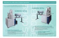
Performance for a wide variety of analytical requirements The all-in-one Schottky SEM SU3900/SU3800SE series delivers high-resolution imaging capability for large specimens and variable pressure function versatility. * Picture represents SU3800SE Plus. ・Supports up to 300 mm diameter/130 mm height specimens (available only for SU3900SE/ SE Plus) ・A maximum weight of 5 kg using 5-axis stage (available only for SU3900SE/ SE Plus) ・Variable pressure function is standard. *Picture Includes optional accessories. ・Equipped with a new Schottky optics. Resolution: 0.9 nm/ 30 kV, 2.5 nm/1 kV ・Advanced...
Open the catalog to page 2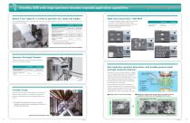
Schottky SEM with large specimen chamber expands application capabilities Robust 5-axis stage for a variety of specimen size, shape and weight Wide Area Camera Navi /SEM MAP The SU3900/SU3800SE series is equipped with a stage that supports large/heavy specimens. A maximum weight of 5 kg can be driven on 5-axis stage. SU3900SE Maximum Specimen size (diameter) Maximum observable range (diameter) Maximum loadable weight *1*2 Maximum loadable height *2 ・The wide-area optical camera image can be smoothly switched to a high-magnification SEM image ・The optical camera image also follows the specimen...
Open the catalog to page 3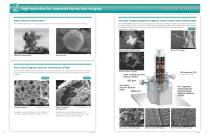
High resolution for improved top-surface imaging High-resolution Observation Versatile imaging capability supports various observation requirements The SU3900/SU3800SE series microscopes are equipped with a new electron gun that allows high-resolution imaging. The SU3900/SU3800SE series microscopes can be equipped with a wide variety of detectors. A diverse range of observation images can be obtained. Detectors include a 4+1-segment Semiconductor backscattered electron detector (BSED) with improved sensitivity suitable for highlighting composition information, and an ultra variable-pressure detector...
Open the catalog to page 4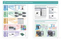
Automation and support functions that improve usa bility ❶ Select Specimen stage ❷ Confirm Specimen height Specimen exchange Specimen exchange sequence offers safety and reliability Supports fast routine measurements ■ Parameters can be called up simply by selecting from a diverse set of parameters. ■Users are able to register and call up their own parameters for each measurement Specimen. Wide range Field of view movement Observation parameter registration screen Camera Navi / SEM MAP covering entire observable region Automatic adjustment Electron beam adjustment Since the observation parameters...
Open the catalog to page 5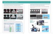
Supporting efficient data acquisition Automatic Wide Area Observation of Semiconductor Devices Uniform Analysis from Preprocessing to Observation Semiconductor devices require support for large specimens, such as chiplet substrates, and observation of specific locations * such as bonds for quality management. Here, we show an example of automatic image capture using EM Flow Creator which is described later. This can reduce manual work by automating routine operations, including identification of bonding areas using a pattern matching function for cross-sectional areas fabricated by ion milling....
Open the catalog to page 6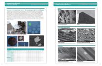
Supporting efficient data acquisition Detection of Foreign Matter During Manufacturing by EDS Particle Analysis Application Gallery Cleanliness control is important when manufacturing automotive parts and lithium-ion batteries. Defect detection by SEM/EDS is widely used for analysis of foreign matter contamination. Below is an example analysis of simulated foreign matter captured by a 47 mm diameter filter. The SU3900SE can load up to 11 sheets of 47 mm diameter filters and can also perform long-duration continuous measurements using the Schottky electron gun which offers excellent irradiation...
Open the catalog to page 7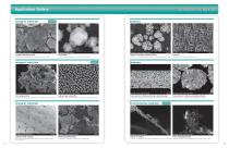
Application Gallery Inorganic materials Tungsten disulfide particles Iron particles Lithium-ion battery cathode material Stacked plate-like particles can be seen at the top surface. The fine particle shape of pure iron can be determined. Distributions of cathode material particles and surrounding binder can be seen. Fine pores in the network can be seen. Inorganic materials Zinc oxide particles High-entropy carbide film Cross section of a lithium-ion battery electrode sheet Cross section of a lithium-ion battery cathode Fine particles with sizes of about 50 nm and 3D shape can be seen. Distribution...
Open the catalog to page 8All Hitachi High-Tech Europe GmbH catalogs and technical brochures
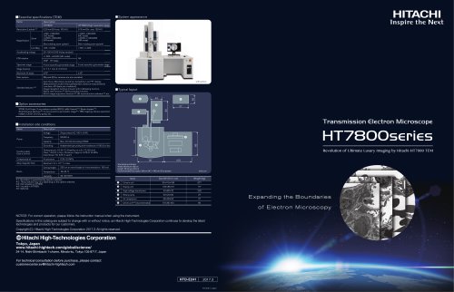 HT7800 Series | TEM
2 Pages

- Hitachi laboratory microscope
- Desktop microscope
- Inspection microscope
- Digital camera microscope
- Measuring microscope
- Hitachi analysis microscope
- Industrial microscope
- Hitachi automated microscope
- Hitachi high-resolution microscope
- Bright field microscope
- Compact microscope
- Materials research microscope
- Metallurgical microscope
- Research microscope
- Quality control microscope
- Dark field microscope
- Ergonomic microscope
- Sample preparation system
- 3D microscope