Si PIN photodiodes S8385/S8729 series
1 /4Pages

Si PIN photodiodes S8385/S8729 series
1 /4Pages
Catalog excerpts

SIP plastic package The S8385/S8729 series is a family of large area Si PIN photodiodes molded into a miniature plastic SIP package (75% smaller in cubic volume than conventional types). Also available are lead forming types that save space when mounted on a PC board. Small plastic package: 4 × 4.8 × 1.8 t mm Barcode scanners 2-pin SIP lead type (lead length: 4.9 mm) High sensitivity, high-speed response Optical switches 2 types of spectral response characteristics available S8385, S8729, S8729-10: for visible to infrared range (λ=320 to 1100 nm) S8729-04: for infrared (λ=760 to 1100 nm) Lead forming type also available (S8729-10) Photosensitive area Structure / Absolute maximum ratings Dimensional outline Effective Photosensitive photosensitive area size area (mm) 2×2 Absolute maximum ratings Power Operating Storage dissipation temperature temperature P Topr Tstg (mW) (°C) (°C) 50 Note) xceeding the absolute maximum ratings even momentarily may cause a drop in product quality. Always be sure to use the E product within the absolute maximum ratings. Electrical and optical characteristics Spectral Peak response sensitivity range wavelength λ λp (nm) 320 to 1100 320 to 1100 760 to 1100 320 to 1100 Short circuit current Isc 100 lx (µA) 4.2 7.5 5 7.5 Cutoff frequency Dark current Temperature Terminal fc ID coefficient of VR=5 V capacitance NEP VR=5 V Ct ID λ=780 nm λ=λp VR=5 V TCID RL=50 Ω f=1 MHz Typ. Max. -3 dB (nA) (nA) (times/°C) (MHz) (pF) (W/Hz1/2) 0.1 1.0 12 1.0 × 10⁻¹⁴ 1.1 × 10⁻¹⁴ 1.15 25 0.2 2.0 16 1.2 × 10⁻¹⁴ 1.1 × 10-
Open the catalog to page 1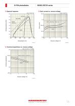
Spectral response Dark current vs. reverse voltage (Typ. Ta=25 °C) Dark current 0.2 erminal capacitance vs. reverse voltage Terminal capacitance vs. reverse voltage (Typ. Ta=25 °C, f=1 MHz) Terminal capacitance
Open the catalog to page 2
Dimensional outline Relative sensitivity Dimensional outlines (unit: mm) S8385, S8729, S8729-04 Photosensitive area a Photosensitive surface Tolerance unless otherwise noted: ±0.1, ±2° Chip position accuracy with respect to the package dimensions marked * X, Y≤±0.2, θ≤±2° Stan
Open the catalog to page 3
Dimensional outline (S8729-10, unit: mm) Photosensitive surface Tolerance unless otherwise noted: ±0.1, ±2° Chip position accuracy with respect to the package dimensions marked * X, Y≤±0.2, θ≤±2° Standard packing: stick (50 pcs/stick) Related information www.hamamatsu.com/sp/ssd/doc_en.html Precautions ∙ Disclaimer ∙ Metal, ceramic, plastic package products Technical information ∙ Si photodiode/Application circuit examples Information described in this material is current as of April 2019. Product specifications are subject to change without prior notice due to improvements or other reasons....
Open the catalog to page 4All HAMAMATSU catalogs and technical brochures
 PHOTON COUTING HEAD
4 Pages
 SPAD MODULES
5 Pages
 LIGHTNINGCURE
29 Pages
 Xenon Flash Lamps
19 Pages
 ORCA-FUSION C14440-20UP
12 Pages
 NanoZommer series
8 Pages
 C13410 series
4 Pages
 C13410-06A
4 Pages
 PMA-12
8 Pages
 L12542
4 Pages
 FLAT EXCIMER
16 Pages
 OPTICAL PINHOLE INSPECTION UNITS
20 Pages
 Optical Gauge series
23 Pages
 L15208-01
3 Pages
 Pulsed Fiber Laser L15187
3 Pages
 L15856-01
3 Pages
 L14001-01
2 Pages
 L11854-336-05
2 Pages
 L14351-02
4 Pages
 LIGHTNINGCURE LC-L1V5
4 Pages
 GC-113A
2 Pages
 Infrared LED L14337-0085R
4 Pages
 Infrared LED L12509 series
9 Pages
 InGaAs camera C12741-11
2 Pages
 InGaAs camera C12741-03
2 Pages
 IMAGEMX2 series
8 Pages
 ORCA-Flash4.0V3 C13440-20CU
4 Pages
 ORCA-Fusion BT
9 Pages
 DIUTHAME
12 Pages
 J12853
2 Pages
 J12432-01
2 Pages
 J10919 SERIES
2 Pages
 Si APD S14644 series
6 Pages
 C15780-401
4 Pages
 CMOS area image sensor S14501
15 Pages
 H15460-40
4 Pages
 R14755U-100
2 Pages
 MPPC modules C14556 series
5 Pages
 Photo IC for rangefinder
14 Pages
 InGaAs APD G14858-0020AA
4 Pages
 Si APD S14124-20
3 Pages
 Si strip detector S13804
3 Pages
 Si photodiode S15289-33
4 Pages
 Si PIN photodiode S15137
4 Pages
 Si PIN photodiode S14605
3 Pages
 Si PIN photodiode S13993
3 Pages
 Si photodiodes S12915 series
4 Pages
 Si photodiode S12742 series
4 Pages
 Si photodiodes S12698 series
5 Pages
 Si PIN photodiode S12271
4 Pages
 Si photodiode S10625-01CT
5 Pages
 Si photodiode S10043
3 Pages
 Si photodiode S9981-01CT
5 Pages
 Si photodiode S9674
5 Pages
 Si photodiodes S9055 series
4 Pages
 Si PIN photodiode S8650
3 Pages
 Si photodiode S8559
3 Pages
 Si photodiodes S8552, S8553
4 Pages
 Si photodiode 8193
3 Pages
 Si photodiode S7686
4 Pages
 Si PIN photodiode S7478
4 Pages
 Si PIN photodiode S4707-01
3 Pages
 Si PIN photodiode S3994-01
3 Pages
 Si PIN photodiode S3759
4 Pages
 Si photodiode S2551
4 Pages
 Si photodiodes S2387 series
4 Pages
 Si photodiodes S2386 series
4 Pages
 Si photodiodes S2281 series
3 Pages
 Si photodiode S1787 series
3 Pages
 Si photodiodes S1337 series
6 Pages
 Si photodiodes S1336 series
6 Pages
 Si photodiodes S1227 series
5 Pages
 Si photodiodes S1226 series
6 Pages
 Si photodiode 16008-33
4 Pages
 Si PIN photodiode S13337-01
4 Pages
 C13398 series
5 Pages
 InGaAs Image sensors
17 Pages
 Thermopile detector T15770
3 Pages
 CMOS linear image sensor S14772
18 Pages
 Si APD S14645 series
6 Pages
 Si APD S14643-02
6 Pages
 One-dimensional PSD S14241
5 Pages
 MEMS mirror S13989-01H
9 Pages
 MEMS mirror S13124-01
10 Pages
 PHOTOMULTIPLIER TUBE R14657
2 Pages
 PHOTON COUNTING HEAD H12775
2 Pages
 MPPC® modules C14452 series
5 Pages
 MEMS-FPI spectrum sensor C14273
11 Pages
 Photodiode modules C10439 series
13 Pages
 Phototransistor S2829
4 Pages
 InGaAs APD G8931 series
4 Pages
 Hamamatsu News 2017 Vol. 1
36 Pages
 Hamamatsu News 2017:Cover Story
36 Pages
 Photomultiplier Tube Modules
76 Pages
 LIGHT SOURCES
23 Pages
 PHOTOTUBES
8 Pages
 FLAME SENSOR UVTRON
4 Pages
 Opto-semiconductor Modules
28 Pages
 PSD
PSD8 Pages
 InGaAs Photodiodes
20 Pages
 Infrared Detectors
36 Pages
 Photo IC
8 Pages
 Image Sensors
48 Pages
 Si Photodiodes
48 Pages
 Si APD
16 Pages
 MPPC®, MPPC modules
34 Pages
 Photonic Devices
44 Pages
 IMAGE INTENSIFIERS
20 Pages
 THERMOELECTRIC COOLED
4 Pages
 FLOW CELLS
4 Pages
 COMPACT HIGH VOLTAGE
2 Pages
 SCANBLOCK C10516
4 Pages
 Immunochromato-Reader C10066
4 Pages
 UV TRONR DRIVING
2 Pages
 PULSE DELAY GENERATOR C10149
4 Pages
 High sensitivity
2 Pages
 FOP (FIBER OPTIC PLATE)
3 Pages
 20 W XENON FLASH LAMP
4 Pages
 UV POWER METERS C6080 SERIES
2 Pages
 Si photodiodes
41 Pages
 Digital CCD Cameras, ORCA-HR
2 Pages


Archived catalogs
 PHOTOSENSOR AMPLIFIER
7 Pages
 FLAT PANEL TYPE
4 Pages
 Microfocus X-ray Sources
2 Pages
 Digital CCD Camera ORCA-HR
2 Pages
 EM-TDI CCD Camera C9100-03
2 Pages
 Infrared LED L10596-02
4 Pages
 Opto-semiconductor Catalog
38 Pages
 2008 Photonic Devices Catalog
32 Pages


- Digital imager
- Visible imager
- CMOS camera module
- Industrial camera module
- ERLO measuring system
- Monitoring camera system
- Full-color camera system
- Microscope
- ERLO screener
- Spectrometer
- USB camera module
- Optical microscope
- Compact imager
- Inspection system
- Inspection imager
- Laboratory microscope
- Photoelectric sensor
- Automatic measurement system
- Optical measurement system
- Rectangular photoelectric sensor