Inverted Emission Microscope iPHEMOS
1 /4Pages

Inverted Emission Microscope iPHEMOS
1 /4Pages
Catalog excerpts
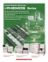
Inverted Emission Microscope Rapidly and precisely localizes semiconductor failure sites through photo emission, thermal emission and laser based techniques. Hamamatsu offers the latest generation of inverted optical analysis tools for simplified direct tester docking and backside wafer probing. Series Tester direct docking type Back side prober type -TD -TP Tester direct docking type -SD
Open the catalog to page 1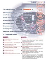
FEATURES OPTIONS NanoLens for high-resolution and high-sensitivity observation Using a NanoLens increases the numerical aperture (N. A.) and drastically improves both resolution and light collection efficiency. This shortens detection time yet delivers high resolution. OBIRCH analysis function The highly popular OBIRCH (Optical Beam Induced Resistance Change) analysis function can be added as an option to detect line defects such as leakage or IDDQ defects. Use of digital lock-in kit enhances the OBIRCH analysis detection functions Digital lock-in by the software ensures a clear and sharp image...
Open the catalog to page 2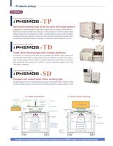
For details on the optional analytical functions and detectors, see the PHEMOS catalog or the various technical notes. High precision backside prober for 300 mm wafers with multiple platforms Equipped with a backside emission prober (BEP) made for 300 mm wafers by SUSS MicroTec. Rapid and accurate multiple pins probing or micro-probing on a wafer enables highly efficient analysis from the backside of a wafer. Its multiple platforms and a full line of options including several laser application options and wafer automatic measurement software offer a wide range of backside analysis. A maximum...
Open the catalog to page 3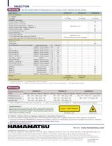
SELECTION SELECTION Hamamatsu Photonics classifies laser diodes, and provides appropriate safety measures and labels according to the classification as required for manufacturers according to IEC 60825-1. When using this product, follow all safety measures according to the IEC. LASER SAFETY CLASS É LASER PRODUCT Description Label Caution Label Cat. No. SSMS0019E10 OCT/2009 HPK Created in Japan Type Name Port for Detector for CAMERA for LASER CAMERA Selection C-CCD Camera : C4880-59 SI-CCD Camera : C11231-02 InGaAs Camera (LN2 cooling ) : C8250-25 1 InGaAs Camera (Peltier cooling) : C8250-26 1...
Open the catalog to page 4All HAMAMATSU catalogs and technical brochures
 PHOTON COUTING HEAD
4 Pages
 SPAD MODULES
5 Pages
 LIGHTNINGCURE
29 Pages
 Xenon Flash Lamps
19 Pages
 ORCA-FUSION C14440-20UP
12 Pages
 NanoZommer series
8 Pages
 C13410 series
4 Pages
 C13410-06A
4 Pages
 PMA-12
8 Pages
 L12542
4 Pages
 FLAT EXCIMER
16 Pages
 OPTICAL PINHOLE INSPECTION UNITS
20 Pages
 Optical Gauge series
23 Pages
 L15208-01
3 Pages
 Pulsed Fiber Laser L15187
3 Pages
 L15856-01
3 Pages
 L14001-01
2 Pages
 L11854-336-05
2 Pages
 L14351-02
4 Pages
 LIGHTNINGCURE LC-L1V5
4 Pages
 GC-113A
2 Pages
 Infrared LED L14337-0085R
4 Pages
 Infrared LED L12509 series
9 Pages
 InGaAs camera C12741-11
2 Pages
 InGaAs camera C12741-03
2 Pages
 IMAGEMX2 series
8 Pages
 ORCA-Flash4.0V3 C13440-20CU
4 Pages
 ORCA-Fusion BT
9 Pages
 DIUTHAME
12 Pages
 J12853
2 Pages
 J12432-01
2 Pages
 J10919 SERIES
2 Pages
 Si APD S14644 series
6 Pages
 C15780-401
4 Pages
 CMOS area image sensor S14501
15 Pages
 H15460-40
4 Pages
 R14755U-100
2 Pages
 MPPC modules C14556 series
5 Pages
 Photo IC for rangefinder
14 Pages
 InGaAs APD G14858-0020AA
4 Pages
 Si APD S14124-20
3 Pages
 Si strip detector S13804
3 Pages
 Si photodiode S15289-33
4 Pages
 Si PIN photodiode S15137
4 Pages
 Si PIN photodiode S14605
3 Pages
 Si PIN photodiode S13993
3 Pages
 Si photodiodes S12915 series
4 Pages
 Si photodiode S12742 series
4 Pages
 Si photodiodes S12698 series
5 Pages
 Si PIN photodiode S12271
4 Pages
 Si photodiode S10625-01CT
5 Pages
 Si photodiode S10043
3 Pages
 Si photodiode S9981-01CT
5 Pages
 Si photodiode S9674
5 Pages
 Si photodiodes S9055 series
4 Pages
 Si PIN photodiode S8650
3 Pages
 Si photodiode S8559
3 Pages
 Si photodiodes S8552, S8553
4 Pages
 Si photodiode 8193
3 Pages
 Si photodiode S7686
4 Pages
 Si PIN photodiode S7478
4 Pages
 Si PIN photodiode S4707-01
3 Pages
 Si PIN photodiode S3994-01
3 Pages
 Si PIN photodiode S3759
4 Pages
 Si photodiode S2551
4 Pages
 Si photodiodes S2387 series
4 Pages
 Si photodiodes S2386 series
4 Pages
 Si photodiodes S2281 series
3 Pages
 Si photodiode S1787 series
3 Pages
 Si photodiodes S1337 series
6 Pages
 Si photodiodes S1336 series
6 Pages
 Si photodiodes S1227 series
5 Pages
 Si photodiodes S1226 series
6 Pages
 Si photodiode 16008-33
4 Pages
 Si PIN photodiode S13337-01
4 Pages
 C13398 series
5 Pages
 InGaAs Image sensors
17 Pages
 Thermopile detector T15770
3 Pages
 CMOS linear image sensor S14772
18 Pages
 Si APD S14645 series
6 Pages
 Si APD S14643-02
6 Pages
 One-dimensional PSD S14241
5 Pages
 MEMS mirror S13989-01H
9 Pages
 MEMS mirror S13124-01
10 Pages
 PHOTOMULTIPLIER TUBE R14657
2 Pages
 PHOTON COUNTING HEAD H12775
2 Pages
 MPPC® modules C14452 series
5 Pages
 MEMS-FPI spectrum sensor C14273
11 Pages
 Photodiode modules C10439 series
13 Pages
 Phototransistor S2829
4 Pages
 InGaAs APD G8931 series
4 Pages
 Hamamatsu News 2017 Vol. 1
36 Pages
 Hamamatsu News 2017:Cover Story
36 Pages
 Photomultiplier Tube Modules
76 Pages
 LIGHT SOURCES
23 Pages
 PHOTOTUBES
8 Pages
 FLAME SENSOR UVTRON
4 Pages
 Opto-semiconductor Modules
28 Pages
 PSD
PSD8 Pages
 InGaAs Photodiodes
20 Pages
 Infrared Detectors
36 Pages
 Photo IC
8 Pages
 Image Sensors
48 Pages
 Si Photodiodes
48 Pages
 Si APD
16 Pages
 MPPC®, MPPC modules
34 Pages
 Photonic Devices
44 Pages
 IMAGE INTENSIFIERS
20 Pages
 THERMOELECTRIC COOLED
4 Pages
 FLOW CELLS
4 Pages
 COMPACT HIGH VOLTAGE
2 Pages
 SCANBLOCK C10516
4 Pages
 Immunochromato-Reader C10066
4 Pages
 UV TRONR DRIVING
2 Pages
 PULSE DELAY GENERATOR C10149
4 Pages
 High sensitivity
2 Pages
 FOP (FIBER OPTIC PLATE)
3 Pages
 20 W XENON FLASH LAMP
4 Pages
 UV POWER METERS C6080 SERIES
2 Pages
 Si photodiodes
41 Pages
 Digital CCD Cameras, ORCA-HR
2 Pages


Archived catalogs
 PHOTOSENSOR AMPLIFIER
7 Pages
 FLAT PANEL TYPE
4 Pages
 Microfocus X-ray Sources
2 Pages
 Digital CCD Camera ORCA-HR
2 Pages
 EM-TDI CCD Camera C9100-03
2 Pages
 Infrared LED L10596-02
4 Pages
 Opto-semiconductor Catalog
38 Pages
 2008 Photonic Devices Catalog
32 Pages


- Digital imager
- Visible imager
- CMOS camera module
- Industrial camera module
- ERLO measuring system
- Monitoring camera system
- Full-color camera system
- ERLO screener
- Spectrometer
- USB camera module
- Optical microscope
- Compact imager
- Inspection system
- Inspection imager
- Laboratory microscope
- Photoelectric sensor
- Automatic measurement system
- Optical measurement system
- Rectangular photoelectric sensor