- Catalogs
- HaiNan Neocrystech Co., Ltd
- Semiconductor / integrated circuits
Semiconductor / integrated circuits
1 /1Page
Semiconductor / integrated circuits
1 /1Page
Catalog excerpts

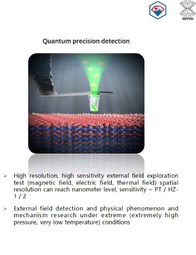
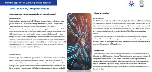
Industrial applications-Quantum precision detection Magneresistance random memory production line quality control Industry shortage: Magnetoresistance random memory' (MRAM) is a new memory technology with magnetic tunnel junction as the unit art. MRAM. with the density of dynamic RAM static RAM. speed and nonvolatile flash memory', is expected to become the next generation of new memory. To integrate nano-sized magnetic tunnel junctions in practical applications, a nanomagnetic field characterization has to be developed technology. One of the main challenges in the characterization of ferromagnetic nanostructures is the need to measure the magnetic field generated by a single nanagnetic structure, however the magnetic signal output by single nanostructures is often smaller than the lower limit of detection of most conventional magnetometers. In addition, measuring large array-type nanomagnetic structures requires complex and high-cost pre-processing processes, and the final measured signal may also have statistical errors, which cannot accurately characterize the characteristics of individual nanomagnetic structures. Empowered value: Magnetic imaging techniques based on quantum precision measurement are expected to detect the magnetic field fraction of individual nanomagnetic structures. Cloth, combined with a varying external magnetic field, is able to measure the magnetic reversal properties of nanoelements. This technique enables quantitative, nondestructive magnetic field detection of nanoscale materials and has the potential to become a common tool for characterizing nanomagnetic structures in MRAM Industry shortage: With the development of the semiconductor industiy, integrated circuit chips, as Moores Law predicts, have integration with Performance is constantly improving. For smaller and smaller units and devices, failure analysis and mispositioning are also becoming more difficult. Meanwhile, the complexity of 3 D microelectronics packaging introduces more potential failure sites, such as different cores, assembly layers, or interconnection between layers, and the detection of these failure sites is a significant challenge. Traditional detection methods such as voltammetry analysis cannot accurately locate the failure location, and beam induction. The technology such as resistance change and micro-light microscopy are not well adapted and the equipment is expensive, and they need certain light transmittance, which cannot meet the requirements of 3D chip detection. Empowered value: The failure analysis technology based on the principle of quantum precision measurement can detect different layers and different layers of the chip. The distribution of the current, can also reconstruct the density distribution of individual PX node carriers. Furthermore, the technology can detect the temperature distribution of the thermal chip surface, reconstruct the electric field information inside the device, realize multi-physical field imaging, and then locate the chip failure site. Therefore, quantum precision measurement technology can be used in chip design and development to improve the quality of chips.
Open the catalog to page 1All HaiNan Neocrystech Co., Ltd catalogs and technical brochures
 Product brochure
18 Pages
Archived catalogs
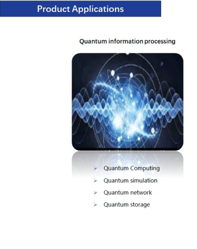
 Quantum simulation
1 Page
 Mineral exploration
1 Page
 Single-sell MRI
1 Page
 Pv device detection
1 Page
 New Energy
1 Page
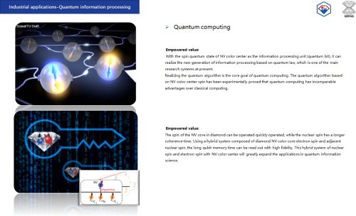 Quantum computing
1 Page
 Management of power grid
1 Page
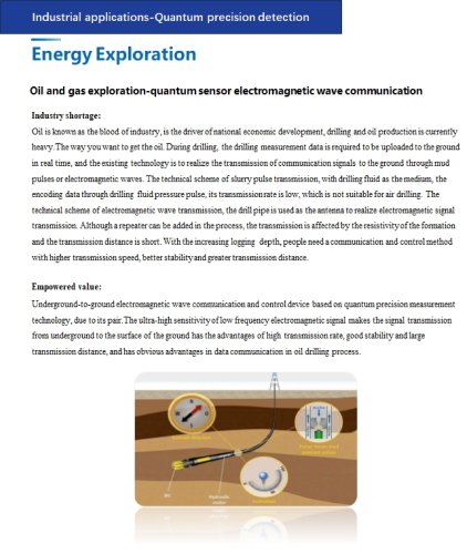 Energy Exploitation
1 Page