


- Products
- Catalogs
- News & Trends
- Exhibitions
MBF200 Solid State Fingerprint Sensor data sheet

MBF200 Solid State Fingerprint Sensor data sheet
- Computer and network security
- Portable and mobile device security
- Access control for doors, locks, and safes
- ID tokens and Smart Cards
- Transportation and medical security
- Finance: secure transactions
The Fujitsu MBF200 is a 500 DPI 8-bit grayscale solid-state capacitive fingerprint sensor. It features a 256 x 300 pixel array with a sensing area of 12.8mm x 15.0mm. The sensor uses a metal electrode and a finger as capacitor plates, with a passivation layer providing resistance. The capacitance is measured and converted into an 8-bit grayscale image.
- Rugged, high-resolution sensor with 500 DPI
- Large image area and programmable gain
- Compact LQFP package with USB, MCU, and SPI interfaces
- Durable with ESD certification and wide operating temperature range
- Integrated 8-bit ADC and auto finger-detection
- Low power consumption
The sensor operates with a 256 x 300 sensor array, capturing fingerprint images one row at a time. The process involves pre-charging and discharging sensor plates, with the difference in voltages indicating capacitance. Sensitivity is adjustable via discharge current and time.
- Microprocessor and SPI bus interfaces
- USB interface with internal and external ROM options
- Various register commands for SPI slave mode
- Recommended solder reflow profile and parts handling
- Guidelines for mechanical design and PCB orientation
The MBF200 is RoHS compliant, ensuring reduced hazardous materials.
- Microprocessor Bus Interface Mode: Utilizes pins like D[7:0], A0, RD, WR, CS0, CS1, EXTINT, INTR, and WAIT. It supports indexed addressing for function registers and disables SPI and USB interfaces.
- SPI Slave Mode: Uses SCLK, SCS, MOSI, MISO, and EXTINT pins. It supports SPI modes (0,0) and (1,1) with data transfer rates up to 12 Mbits per second.
- USB Interface Mode: Utilizes DP, DM, EXTINT, XTAL1, and XTAL2 pins. It requires a 12 MHz clock source and accesses internal USB descriptor ROM for communication.
- CTRLA: Initiates image conversion and selects input sources for the A/D converter.
- CTRLB: Manages A/D converter status and automatic finger detection.
- CTRLC: Controls general output port pins P0 and P1.
- Get Row: Load the row address, initiate a GETROW operation via CTRLA, and read CTRLA 256 times to retrieve data.
- Get Whole Image: Initiate with CTRLA, no pre-loading of row/column registers needed, and automatically starts A/D conversion.
- Get Sub-Image: Load starting and ending addresses for rows and columns, initiate with CTRLA, and read until the sub-image is retrieved.
- Microprocessor Mode: Uses specific register writes and reads for operations.
- SPI Mode: Commands are sent via MOSI and data read via MISO, requiring separate commands for each row.
- USB Mode: Operations initiated on endpoint 0, with image data read from endpoint 1.
- Absolute Maximum Ratings: Includes power supply voltage, output current, and storage temperature limits.
- Operating Range: Specifies supply voltage and ambient temperature ranges.
- DC Characteristics: Details input/output voltage levels and leakage currents for different VDD values.
- Power Supply Consumption: Lists typical and maximum current consumption for various modes and conditions.
- Provides timing specifications for read and write cycles in microprocessor and SPI modes.
- Dimensions: Details the physical dimensions of the sensor package.
- Recommended Land Pattern: Provides dimensions for PCB design.
- Array Orientation: Specifies pin layout and sensor array coordinates.
- Technical Recommendations: Includes solder reflow profiles, handling, and storage conditions.
- Power and Ground Connections: To minimize image noise, connect VDDA1 and VDDA2 (analog power supply pins) with a bulk capacitor (4.7µF to 10µF) and two 0.1µF capacitors in parallel to ground. Separate these from digital power pins using a 10Ω resistor. For digital power pins (VDD1, VDD2, VDD3), place 0.1µF capacitors close to the pins. Input signals tied high should connect through a 1K to 10KΩ resistor for ESD protection.
- Sensor PCB Orientation: Mount the MBF200 with pins 1-40 pointing away from the user and pins 41-80 towards the user. Ensure the sensor is flush with the surface for optimal finger contact. A groove or channel is recommended for proper finger positioning.
- The MBF200 sensor complies with RoHS standards, with no hazardous substances like asbestos, azo colorants, or ozone-depleting substances detected.
- 2001 V.1.0: Initial Release
- 2004 V.1.1: Package specification and typo corrections
- 2005 V.1.2: Updates on cover page, lead-free classification, power consumption values, and addition of technical recommendations and RoHS compliance table
- 2005 V.1.3: Solder reflow profile update
Catalog excerpts
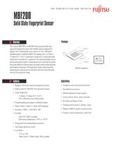
Computer access and network securityՕPortable device security Mobile fingerprint image capture ՕAccess control: doors, locks, and safes ID tokens and Smart Cards ՕTransportation security: vehicles, cargo Medical: HIPAA, patient records privacy ՕFinance: secure transactions, audit trail > The Fujitsu MBF200 is a 500 DPI 8-bit grayscale solid-state capacitive fingerprint sensor that reliably captures fingerprint images. The 2-dimensional array consists of 256 x 300 pixels manufactured in standard CMOS. The sensing area is 12.8mm x 15.0mm (0.5" x 0.6"). Each pixel is made up of a metal electrode, which acts as one plate of a capacitor. The contacting finger acts as the second capacitor plate. A passivation layer on the device surface forms the dielectric between these two plates and provides abrasion and chemical resistance. The fingerprint image is determined by measuring the capacitance at each pixel and converting that data into an 8-bit grayscale image. > Rugged, solid-state capacitive fingerprint sensorՕHigh resolution 500 DPI, 8-bit grayscale imager Large image area:Ֆ12.8mm x 15.0mm (0.5" x 0.6") 256 x 300 pixel array (50um pitch)֕Programmable gain adapts to different fingersSmall: 24mm x 24mm x 1.4mm LQFP package ՕInterfaces: USB1.1, 8-bit MCU, SPI Durable:ՖESD: FCC-B/CE certifiedOperating temperature: -20ְC to +85CЕIntegrated 8-bit analog-digital converterAuto finger-detection circuit ՕLow Power3.3V to 5.0V֖20mA active, <200A sleep, 20յA standby >
Open the catalog to page 1
Fujitsu Microelectronics America, Inc. 3 > Pin Number 1VDDA1PWRAnalog Power Supply2VSSA1GNDAnalog Ground 3ISETOSets Reference Current 4AINIAnalog Input 5FSETOSets Internal Multi-vibrator Frequency 6VSSA2GNDAnalog Ground 7VDDA2PWRAnalog Power Supply 8TESTITest Mode Enable 9P0O8mA4mAOutput Port 010P1O8mA4mAOutput Port 1 11D7I/O8mA4mAData Bit 7 12D6I/O8mA4mAData Bit 6 13D5I/O8mA4mAData Bit 5 14D4I/O8mAData Bit 4 15VSS1GNDDigital Ground 16VDD1PWRDigital Power Supply 17D3I/O8mA4mAData Bit 3 18D2I/O8mA4mAData Bit 2 19D1I/O8mA4mAData Bit 1 20D0I/O8mA4mAData Bit 0 21A0IAddress Input 22RD > Name Type...
Open the catalog to page 6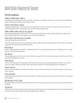
4 Fujitsu Microelectronics America, Inc. VDDA1, VDDA2 (Pins 1 and 7) > Power Supply to the analog section of the sensor. VDDA1 powers the array, row drivers, column receivers, A/D converter, and sample/hold amplifier. VDDA2 powers the multi-vibrator and bias circuits. VSSA1, VSSA2 (Pins 2 and 6) > Ground for the analog section of the sensor. VSSA1 is the ground return for the array, row drivers, column receivers, A/D converter, and sample hold amplifier. VSSA2 is the ground return for the multi-vibrator and bias circuits. VDD1, VDD2, VDD3 ( Pins 25, 16, and 39) > Power supply to the digital logic...
Open the catalog to page 7
Fujitsu Microelectronics America, Inc. 5 Read enable, active low. To read from the chip, drive RD > Write enable, active low. To write to the chip, drive WR > Chip select, active low. The CS0 > Chip select, active high. The CS1/SCLK pin has a weak latch that holds the pins state when not being driven. CS1/SCLK may be left unconnected in USB mode if not using an external serial ROM. The function of this pin depends on the MODE1 and MODE0 pins. > CS1/SCLK functions as an active-high chip select input. Drive CS1/SCLK high while CS0-/CSC- is low to select the chip. > CS1/SCLK functions as the slave...
Open the catalog to page 8
6 Fujitsu Microelectronics America, Inc. Wait output, active low. W > SPI Master Output/Slave input. The MOSI pin has a weak latch that holds the pins state when not being driven. MOSI may be left unconnected in MCU mode or USB mode if not using an external serial ROM. The function of this pin depends on the MODE1 and MODE0 pins. > MOSI functions as the slave serial input. > MOSI functions as the master serial data output to the slave serial ROM data input. Unlike standard SPI, MOSI is actively driven high and low when transmitting data and is high impedance when idle. Connect a pull-up resistor...
Open the catalog to page 9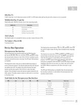
Fujitsu Microelectronics America, Inc. 7 USB D- data line. Use 43 ohm series resistor. In MCU or SPI mode, either pull-up this pin with a resistor or tie it to ground. > Mode Select pins. MODE[1:0] select one of four operating modes. > Test Mode Enable. It is intended for factory use only. Connect this pin to VSS. > Unconnected pins. > MODE[1:0] 00bMicroprocessor Bus Mode01bSPI Bus Mode 10bUSB Mode, Using Internal ROM 11bUSB Mode, Using External ROM CS0 H X X X X De-selected High ImpedanceX L X X XDe-selected High ImpedanceL H X H H Standby High Impedance L H L L H Read Index Register Output...
Open the catalog to page 10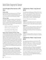
8 Fujitsu Microelectronics America, Inc. SPI (Slave) bus mode uses the following pins: SCLK, SCS > In SPI Slave Mode, the sensor can operate in either SPI mode (0, 0) where CPOL = 0 and CPHA = 0 or SPI mode (1, 1) where CPOL = 1 and CPHA = 1. The SPI Master may clock in commands and clock out data up to 12 Mbits per second. The SPI Master can write and read the registers of the sensor even when the internal 12 MHz multivibrator or XTAL1/XTAL2 oscillator is halted.MOSI bits are sampled on the rising edge of SCK ՕMISO bits change on the falling edge of SCK SCK can be idle in either a high or low...
Open the catalog to page 11
Fujitsu Microelectronics America, Inc. 9 > Index 0x00RAHRow Address, HighR/W0x01RALRow Address, LowR/W 0x02CALColumn Address, LowR/W 0x03REHRow Address End, HighR/W 0x04RELRow Address End, LowR/W 0x05CELColumn Address End, LowR/W 0x06DTRDischarge Time RegisterR/W 0x07DCRDischarge Current RegisterR/W 0x08CTRLAControl Register AR/W 0x09CTRLBControl Register BR/W0x0ACTRLCControl Register CR/W 0x0BSRAStatus Register AR0x0CPGCProgrammable Gain Control RegisterR/W 0x0DICRInterrupt Control RegisterR/W0x0EISRInterrupt Status RegisterR/W 0x0FTHRThreshold RegisterR/W 0x10CIDHChip Identification, HighR...
Open the catalog to page 12
10 > Fujitsu Microelectronics America, Inc. Bit Number [7:0] RA[7:0] Low eight bits of Row Address Register Bit Number [7:0] CA[7:0] Column Address Register Bit Number [7:1] - Reserved. Write 0 to these bits.0 REND[8] Most Significant Bit of Row Address Register Bit Number [7:0] REND[7:0] Low eight bits of Row Address Register Bit Number [7:0] CEND[7:0] Column Address Register > Bit Name Function Bit Name Function Bit Name Function Bit Name Function Bit Name Function >
Open the catalog to page 13All Fujitsu catalogs and technical brochures
 STYLISTIC Q7310
2 Pages
 LIFEBOOK U9310
2 Pages
 LIFEBOOK E5410
2 Pages
 FUJITSU Tablet LIFEBOOK T939
8 Pages
 Fujitsu LIFEBOOK S938
6 Pages
 FUJITSU Workstation CELSIUS
2 Pages
 LIFEBOOK U7 Family
2 Pages
 FUJITSU Workstation CELSIUS R970
10 Pages
 From edge to core to cloud
8 Pages
 Online Storage Systems
2 Pages
 Data-Centric Storage
10 Pages
 CONTROL SYSTEM & OPTIONAL PARTS
28 Pages
 MULTI SPLIT
26 Pages
 PRIMEFLEX Cluster-in-a-box
2 Pages
 rx1330-m3
11 Pages
 rx2510-m2
10 Pages
 LIFEBOOK-S937
6 Pages
 ESPRIMO-X923-T
8 Pages
 ESPRIMO-X956-T
8 Pages
 Data sheet - PRIMERGY RX2530 M1
12 Pages
 Data sheet - PRIMERGY RX2540 M1
11 Pages
 Data sheet - PRIMERGY RX2520 M1
11 Pages
 ETERNUS JX40 S2
5 Pages
 ETERNUS DX60 S3
6 Pages
 ETERNUS JX40
5 Pages
 ETERNUS DX200 S3
6 Pages
 ETERNUS DX100 S3
6 Pages
 PRIMEQUEST 2800B
8 Pages
 PRIMEQUEST 2800B2
8 Pages
 PRIMEQUEST 2400E2
9 Pages
 PRIMEQUEST 2800E2
8 Pages
 FUJITSU Enterprise
138 Pages
 1800E
1800E9 Pages
 PRIMEQUEST 2400E
9 Pages
 PRIMEQUEST 2800E
10 Pages
 Fujitsu Mainboard D3162-B
3 Pages
 Fujitsu Mainboard D3128-B
3 Pages
 Fujitsu Mainboard D3243-S
3 Pages
 Fujitsu Mainboard D3231-S
3 Pages
 Fujitsu Mainboard D3235-S
3 Pages
 Fujitsu Mainboard D3236-S
3 Pages
 Fujitsu Mainboard D3313-S
3 Pages
 Fujitsu Mainboard D3003-S
3 Pages
 Fujitsu Mainboard D3071-S
3 Pages
 Fujitsu Mainboard D3076-S
3 Pages
 Fujitsu Mainboard D3230-B
3 Pages
 Fujitsu Mainboard D3221-B
3 Pages
 Fujitsu Mainboard D3220-B
3 Pages
 Fujitsu Mainboard D2990-A
3 Pages
 Fujitsu Mainboard D2991-A
3 Pages
 Fujitsu Mainboard D3161-B
3 Pages
 BroadOne GX4000 Series
4 Pages
 ds-fts-primequest1800e2
7 Pages
 ds-primequest2800b
8 Pages
 ETERNUS DX8700 S2
5 Pages
 PRIMEQUEST 1800E2
10 Pages
 Microcontroller
36 Pages
 FerVID family FRAM RFID LSI
4 Pages
 FRAM (All Products Catalog)
4 Pages
 FCRAM (All Products Catalog)
4 Pages
 Fujitsu Automotive Solutions
9 Pages
 FUJITSU SEMICONDUCTOR LIMITED
10 Pages
 test
test3 Pages




![Microcontroller [All Products Catalog]](https://img.directindustry.com/pdf/repository_di/34295/microcontroller-all-products-catalog-20296_1mg.jpg)
Archived catalogs
 VCO (800 to 2500 MHz)
12 Pages
![Product Guide [Microcomputer]](https://img.directindustry.com/pdf/repository_di/34295/product-guide-microcomputer-107851_1mg.jpg) Product Guide [Microcomputer]
Product Guide [Microcomputer]332 Pages
 FUJITSU SEMICONDUCTOR LIMITED
10 Pages
![FRAM [All Products Catalog]](https://img.directindustry.com/pdf/repository_di/34295/fram-all-products-catalog-19956_1mg.jpg) FRAM [All Products Catalog]
FRAM [All Products Catalog]4 Pages
 Power Management ICs
16 Pages
 FUJITSU MICROELECTRONICS LIMITED
10 Pages
 H.264 CODEC factsheet
1 Page
 Enhancing System Solutions
12 Pages
 Mobile WiMAX SoC Fact Sheet
2 Pages
 Networking ASSP Solutions
2 Pages
 WiMAX: MB87M3400 Fact Sheet
4 Pages
 MB91F465XA-factsheet
2 Pages


![Product Guide [ ASSP•Memory•ASIC ]](https://img.directindustry.com/pdf/repository_di/34295/product-guide-assp-memory-asic-107849_1mg.jpg)


- Ethernet switch
- LCD screen
- Industrial monitor
- Automation software solution
- Management software solution
- Intel® Core™ PC
- Fujitsu HDMI monitor
- Fujitsu VESA mounting monitor
- USB 2.0 PC
- Windows PC
- Process software
- Real-time software
- LED monitor
- SATA PC
- USB monitor
- USB PC
- Control software
- Compact PC
- RJ45 PC
- Monitoring software solution