Catalog excerpts
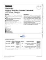
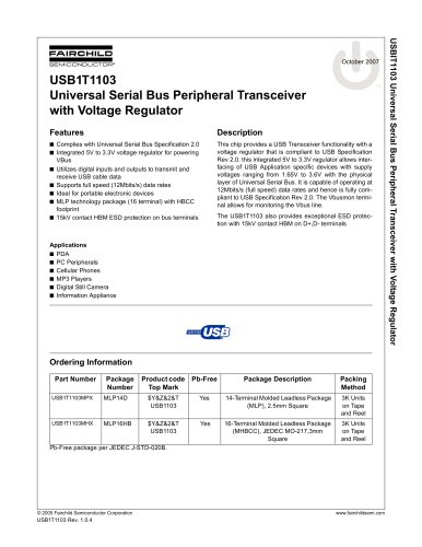
© 2005 Fairchild Semiconductor Corporation www.fairchildsemi.com USBIT1103 Universal Serial Bus Peripheral Transceiver with Voltage Regulator October 2007 USB1T1103 Rev. 1.0.4 USB1T1103 Universal Serial Bus Peripheral Transceiver with Voltage Regulator Features ¡ Complies with Universal Serial Bus Specification 2.0 ¡ Integrated 5V to 3.3V voltage regulator for powering VBus ¡ Utilizes digital inputs and outputs to transmit and receive USB cable data ¡ Supports full speed (12Mbits/s) data rates ¡ Ideal for portable electronic devices ¡ MLP technology package (16 terminal) with HBCC footprint ¡ 15kV contact HBM ESD protection on bus terminals Applications ¡ PDA ¡ PC Peripherals ¡ Cellular Phones ¡ MP3 Players ¡ Digital Still Camera ¡ Information Appliance Description This chip provides a USB Transceiver functionality with a voltage regulator that is compliant to USB Specification Rev 2.0. this integrated 5V to 3.3V regulator allows interfacing of USB Application specific devices with supply voltages ranging from 1.65V to 3.6V with the physical layer of Universal Serial Bus. It is capable of operating at 12Mbits/s (full speed) data rates and hence is fully compliant to USB Specification Rev 2.0. The Vbusmon terminal allows for monitoring the Vbus line. The USB1T1103 also provides exceptional ESD protection with 15kV contact HBM on D+,D- terminals Ordering Information Pb-Free package per JEDEC J-STD-020B. Part Number Package Number Product code Top Mark Pb-Free Package Description Packing Method USB1T1103MPX MLP14D $Y&Z&2&T USB1103 Yes 14-Terminal Molded Leadless Package (MLP), 2.5mm Square 3K Units on Tape and Reel USB1T1103MHX MLP16HB $Y&Z&2&T USB1103 Yes 16-Terminal Molded Leadless Package (MHBCC), JEDEC MO-217,3mm Square 3K Units on Tape and Reel
Open the catalog to page 1
USB1T1103 Universal Serial Bus Peripheral Transceiver with Voltage Regulator © 2005 Fairchild Semiconductor Corporation www.fairchildsemi.com USB1T1103 Rev. 1.0.4 2 Typical Application Figure 1. Logic Diagram Connection Diagrams Figure 2. MLP16 GND Exposed Diepad (Bottom View) Figure 3. MLP14 GND Exposed Diepad (Bottom View)
Open the catalog to page 2
USB1T1103 Universal Serial Bus Peripheral Transceiver with Voltage Regulator © 2005 Fairchild Semiconductor Corporation www.fairchildsemi.com USB1T1103 Rev. 1.0.4 3 Terminal Descriptions Terminal Number Terminal Name I/O Terminal Description MLP14 MLP16 1 1 OE I Output Enable: Active LOW enables the transceiver to transmit data on the bus. When not active the transceiver is in the receive mode (CMOS level is relative to VCCIO) 2 2 RCV O Receive Data Output: Non-inverted CMOS level output for USB differential Input (CMOS output level is relative to VCCIO). Driven LOW when SUSPN is HIGH; RCV...
Open the catalog to page 3
USB1T1103 Universal Serial Bus Peripheral Transceiver with Voltage Regulator © 2005 Fairchild Semiconductor Corporation www.fairchildsemi.com USB1T1103 Rev. 1.0.4 4 Functional Description The USB1T1103 transceiver is designed to convert CMOS data into USB differential bus signal levels and to convert USB differential bus signal to CMOS data. To minimize EMI and noise the outputs are edge rate controlled with the rise and fall times controlled and defined for full speed data rates only (12Mbits/s). The rise, fall times are balanced between the differential terminals to minimize skew. The...
Open the catalog to page 4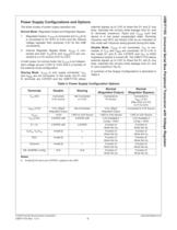
USB1T1103 Universal Serial Bus Peripheral Transceiver with Voltage Regulator © 2005 Fairchild Semiconductor Corporation www.fairchildsemi.com USB1T1103 Rev. 1.0.4 5 Power Supply Configurations and Options The three modes of power supply operation are: Normal Mode: Regulated Output and Regulator Bypass 1. Regulated Output: VCCIO is connected and VCC(5.0) is connected to 5V (4.0V to 5.5V) and the internal voltage regulator then produces 3.3V for the USB connections. 2. Internal Regulator Bypass Mode: VCCIO is connected and both VCC(5.0) and VREG(3.3) are connected to a 3.3V source (3.0V to...
Open the catalog to page 5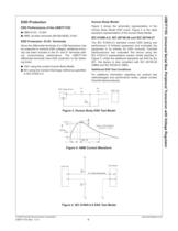
USB1T1103 Universal Serial Bus Peripheral Transceiver with Voltage Regulator © 2005 Fairchild Semiconductor Corporation www.fairchildsemi.com USB1T1103 Rev. 1.0.4 6 ESD Protection ESD Performance of the USB1T1103 ¡ HBM D+/D-: 15.0kV ¡ HBM, all other terminals (Mil-Std 883E): 6.5kV ESD Protection: D+/D- Terminals Since the differential terminals of a USB transceiver may be subjected to extreme ESD voltages, additional immunity has been included in the D+ and D- terminals without compromising performance. The USB1T1103 differential terminals have ESD protection to the following limits: ¡ 15kV...
Open the catalog to page 6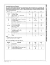
USB1T1103 Universal Serial Bus Peripheral Transceiver with Voltage Regulator © 2005 Fairchild Semiconductor Corporation www.fairchildsemi.com USB1T1103 Rev. 1.0.4 7 Absolute Maximum Ratings The .Absolute Maximum Ratings. are those values beyond which the safety of the device cannot be guaranteed. The device should not be operated at these limits. The parametric values defined in the Electrical Characteristics tables are not guaranteed at the absolute maximum ratings. The .Recommended Operating Conditions. table defines the conditions for actual device operation. Notes: 7. IO Absolute...
Open the catalog to page 7
USB1T1103 Universal Serial Bus Peripheral Transceiver with Voltage Regulator © 2005 Fairchild Semiconductor Corporation www.fairchildsemi.com USB1T1103 Rev. 1.0.4 8 DC Electrical Characteristics Supply Terminals Over recommended range of supply voltage and operating free air temperature (unless otherwise noted). VCC (5V) = 4.0V to 5.5V or VREG (3.3V) = 3.0V to 3.6V, VCCIO = 1.65V to 3.6V. Notes: 9. ILOAD includes the pull-up resistor current via terminal VPU 10. The minimum voltage in Suspend mode is 2.7V. 11. Not tested in production, value based on characterization. 12. Excludes any...
Open the catalog to page 8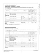
USB1T1103 Universal Serial Bus Peripheral Transceiver with Voltage Regulator © 2005 Fairchild Semiconductor Corporation www.fairchildsemi.com USB1T1103 Rev. 1.0.4 9 DC Electrical Characteristics Digital Terminals . excludes D+, D- Terminals Over recommended range of supply voltage and operating free air temperature (unless otherwise noted). VCCIO = 1.65V to 3.6V. Notes: 16. If VCCIO VREG, leakage current is higher than specified. DC Electrical Characteristics Analog I/O Terminals . D+, D- Terminals Over recommended range of supply voltage and operating free air temperature (unless otherwise...
Open the catalog to page 9All Fairchild Semiconductor catalogs and technical brochures
-
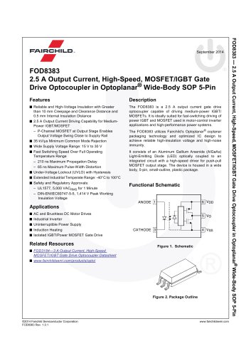
FOD8383 2.5 A Output Current
18 Pages
-
Logic SELECTION GUIDE
12 Pages
-
Automotive Solutions Guide
8 Pages
-
Motor Drive Solution Guide
20 Pages
-
Mobile Solutions Guide
40 Pages
-
AUTOMOTIVE SOLUTIONS
16 Pages
-
Power Solutions Guide
60 Pages
-
STANDARD PRODUCTS GUIDE
72 Pages
Archived catalogs
-
3:1 Analog Switch Products
2 Pages
-
USB Multimedia Switches
2 Pages
-
Analog switch & interface
12 Pages
-
Mobile overview
4 Pages
-
TinyLogic® Product Overview
4 Pages
-
Optocoupler Solutions
24 Pages
-
Motor DRIVE solutions
32 Pages
-
LED LIGHTING SOLUTIONS
16 Pages
-
DIGITAL DISPLAY SOLUTIONS
36 Pages
-
RENEWABLE ENERGY SOLUTIONS
32 Pages
-
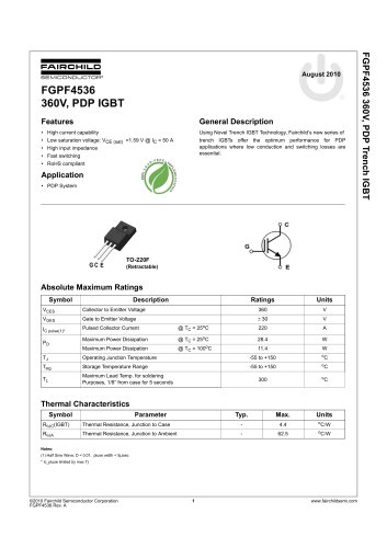
FGPF4536 360V, PDP IGBT
8 Pages
-
FSAR001B AC-DC Linear Regulator
12 Pages
-
Fairchild - Power solutions
52 Pages

