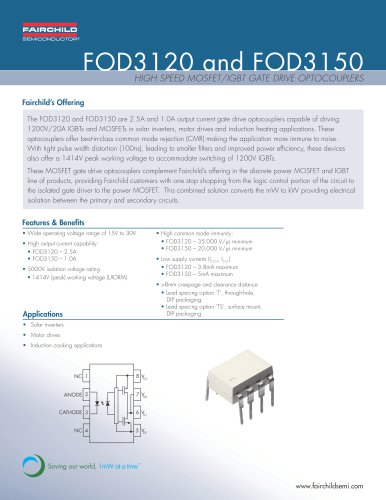
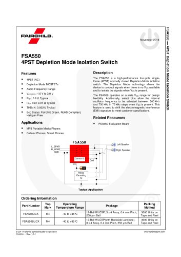
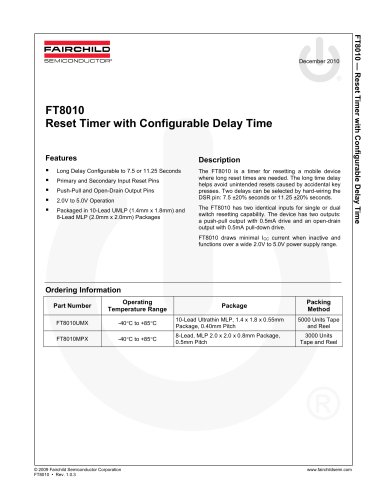
Catalog excerpts

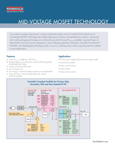
Smart Power Stage (SPS) Portfolio Next-Generation, Multi-Chip Module The SPS module family is a next-generation, ultra-compact, integrated MOSFET plus driver power stage solution. Compared to competitive modules, the family offers three-percent greater efficiency, unique monitoring and protection features, all in 33-percent less space. This family leverages Fairchild’s DrMOS expertise to deliver high efficiency, high-power density and high-switching frequency in applications such as synchronous buck DC-DC converters for high-performance computing and telecom systems. With an integrated approach, the complete switching power stage is optimized for driver and MOSFET dynamic performance, system inductance and power MOSFET RDS(ON). SPS modules use our highperformance PowerTrench® MOSFET technology to reduce ringing, eliminating the need for a snubber circuit in most buck converter applications. Unique Features • Ultra-compact 5 mm x 5 mm x 0.8 mm PQFN with Dual Cool™ packaging technology • Three-state 3.3V PWM and 5V PWM input gate driver • Integrated Zero Cross Detect (ZCD) or FCCM circuitry for better light load efficiency • Dual-mode enable and catastrophic fault reporting pin • Under-voltage lockout (UVLO) protection • Optimized for switching frequencies, up to 2 MHz • Low shutdown current < 3 μA • Improved power stage dynamic performance, system inductance • PowerTrench® MOSFET technology to reduce ringing, eliminate snubber in most buck converter designs • Thermal monitoring, programmable thermal shutdown DC-DC Power Delivery Applications • Servers and workstations • Telecom ASIC power • High-performance notebooks • Game consoles
Open the catalog to page 1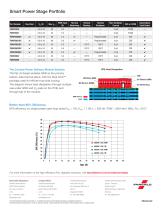
Smart Power Stage Portfolio Part Number Dual Cool Thermal Monitoring Thermal Warning Thermal Shutdown Catastrophic Fault Detect The Coolest Power Delivery Module Solution The flip LS design enables GND as the primary bottom-side thermal plane, with the Dual Cool™ package used for efficient top-side cooling. The diagram shows heat dissipation through multiple vias under GND and VIN pads on the PCB, and through top of the module. SPS Heat Dissipation Clip Q2 Drain (SW) SW Better than 95% Efficiency SPS efficiency on single-phase open loop board VIN = 12V, VOUT = 1.8V, L = 250 nH, FSW = 300...
Open the catalog to page 2All Fairchild Semiconductor catalogs and technical brochures
-
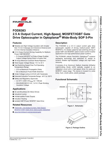
 FOD8383 2.5 A Output Current
18 Pages
-
 Logic SELECTION GUIDE
12 Pages
-
 Automotive Solutions Guide
8 Pages
-
 Motor Drive Solution Guide
20 Pages
-
 Mobile Solutions Guide
40 Pages
-
 AUTOMOTIVE SOLUTIONS
16 Pages
-
 Power Solutions Guide
60 Pages
-
 STANDARD PRODUCTS GUIDE
72 Pages


Archived catalogs
-
 3:1 Analog Switch Products
2 Pages
-
 USB Multimedia Switches
2 Pages
-
 Analog switch & interface
12 Pages
-
 Mobile overview
4 Pages
-
 TinyLogic® Product Overview
4 Pages
-
 Optocoupler Solutions
24 Pages
-
 Motor DRIVE solutions
32 Pages
-
 LED LIGHTING SOLUTIONS
16 Pages
-
 DIGITAL DISPLAY SOLUTIONS
36 Pages
-
 RENEWABLE ENERGY SOLUTIONS
32 Pages
-
 FGPF4536 360V, PDP IGBT
8 Pages
-
 FSAR001B AC-DC Linear Regulator
12 Pages
-
 Fairchild - Power solutions
52 Pages