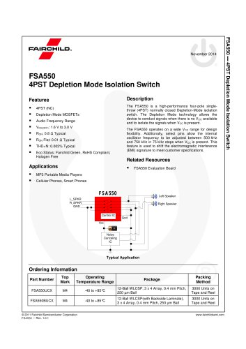
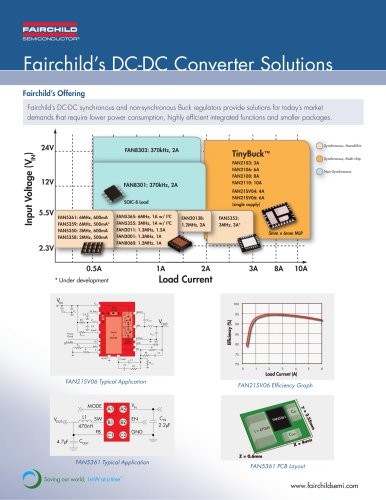
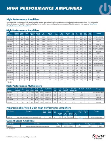
Catalog excerpts
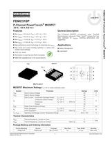
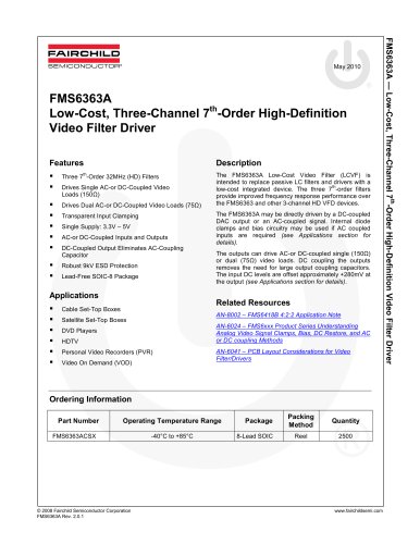
June 2010 ©2010 Fairchild Semiconductor Corporation FDMC510P Rev.C5 1 www.fairchildsemi.com FDMC510P P-Channel PowerTrench® MOSFET FDMC510P P-Channel PowerTrench® MOSFET -20 V, -18 A, 8.0 mÙ Features ..Max rDS(on) = 8.0 mÙ at VGS = -4.5 V, ID = -12 A ..Max rDS(on) = 9.8 mÙ at VGS = -2.5 V, ID = -10 A ..Max rDS(on) = 13 mÙ at VGS = -1.8 V, ID = -9.3 A ..Max rDS(on) = 17 mÙ at VGS = -1.5 V, ID = -8.3 A ..High performance trench technology for extremely low rDS(on) ..High power and current handling capability in a widely used surface mount package ..100% UIL Tested ..Termination is Lead-free and RoHS Compliant ..HBM ESD capability level >2 KV typical (Note 4) General Description This P-Channel MOSFET is produced using Fairchild Semiconductor’s advanced Power Trench® process that has been optimized for rDS(ON), switching performance and ruggedness. Applications ..Battery Management ..Load Switch Bottom D D D D S S S G Top Pin 1 MLP 3.3x3.3 MOSFET Maximum Ratings TA = 25 °C unless otherwise noted Thermal Characteristics Package Marking and Ordering Information Symbol Parameter Ratings Units VDS Drain to Source Voltage -20 V VGS Gate to Source Voltage ±8 V ID Drain Current -Continuous (Package limited) TC = 25 °C -18 A -Continuous (Silicon limited) TC = 25 °C -54 -Continuous TA = 25 °C (Note 1a) -12 -Pulsed -50 EAS Single Pulse Avalanche Energy 37 mJ PD Power Dissipation TC = 25 °C 41 W Power Dissipation TA = 25 °C (Note 1a) 2.3 TJ, TSTG Operating and Storage Junction Temperature Range -55 to +150 °C RèJC Thermal Resistance, Junction to Case 3 °C/W RèJA Thermal Resistance, Junction to Ambient (Note 1a) 53 Device Marking Device Package Reel Size Tape Width Quantity FDMC510P FDMC510P MLP 3.3X3.3 13 ’’ 12 mm 3000 units
Open the catalog to page 1
FDMC510P Rev.C5 2 www.fairchildsemi.com FDMC510P P-Channel PowerTrench® MOSFET Electrical Characteristics TJ = 25 °C unless otherwise noted Off Characteristics On Characteristics Dynamic Characteristics Switching Characteristics Drain-Source Diode Characteristics Symbol Parameter Test Conditions Min Typ Max Units BVDSS Drain to Source Breakdown Voltage ID = -250 ìA, VGS = 0 V -20 V ÄBVDSS ÄTJ Breakdown Voltage Temperature Coefficient ID = -250 ìA, referenced to 25 °C -12 mV/°C IDSS Zero Gate Voltage Drain Current VDS = -16 V, VGS = 0 V -1 ìA IGSS Gate to Source Leakage Current VGS = ±8 V,...
Open the catalog to page 2
FDMC510P Rev.C5 3 www.fairchildsemi.com FDMC510P P-Channel PowerTrench® MOSFET Typical Characteristics TJ = 25 °C unless otherwise noted Figure 1. 0.00.51.01.52.001020304050VGS = -4.5 VVGS = -1.8 V PULSE DURATION = 80 ìsDUTY CYCLE = 0.5%MAXVGS = - 1.5 VVGS = -1.2 VVGS = -2.5 V-ID, DRAIN CURRENT ( A)-VDS, DRAIN TO SOURCE VOLTAGE (V)On Region Characteristics Figure 2. 01020304050012345VGS = -1.8 V PULSE DURATION = 80 ìsDUTY CYCLE = 0.5%MAXNORMALIZEDDRAIN TO SOURCE ON-RESISTANCE-ID, DRAIN CURRENT (A)VGS = -2.5 VVGS = -1.5 VVGS = -1.2 VVGS = -4.5 VNormalized On-Resistance vs Drain Current and...
Open the catalog to page 3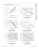
FDMC510P Rev.C5 4 www.fairchildsemi.com FDMC510P P-Channel PowerTrench® MOSFET Figure 7. 0204060801000.01.53.04.5ID = -12 A VDD = -12 VVDD = -8 V-VGS, GATE TO SOURCE VOLTAGE ( V)Qg, GATE CHARGE (nC)VDD = -10 VGate Charge Characteristics Figure 8. 0.11102040010001000020000 f = 1 MHzVGS = 0 VCAPACITANCE ( pF)-VDS, DRAIN TO SOURCE VOLTAGE (V)CrssCossCissCapacitance vs Drain to Source Voltage Figure 9. 0.11101001000110TJ = 100 oC20 TJ = 25 oCTJ = 125 oCtAV, TIME IN AVALANCHE (ms)-IAS, AVALANCHE CURRENT (A)Unclamped Inductive Switching Capability Figure 10. 2550751001251500102030405060VGS = -4.5...
Open the catalog to page 4
FDMC510P Rev.C5 5 www.fairchildsemi.com FDMC510P P-Channel PowerTrench® MOSFET Figure 13. 10-410-310-210-111010010000.0010.010.11SINGLE PULSERèJA = 125 oC/WDUTY CYCLE-DESCENDING ORDERNORMALIZED THERMAL IMPEDANCE, ZèJAt, RECTANGULAR PULSE DURATION ( sec)D = 0.5 0.2 0.1 0.05 0.02 0.012PDMt1t2NOTES:DUTY FACTOR: D = t1/t2PEAK TJ = PDM x ZèJA x RèJA + TAJunction-to-Ambient Transient Thermal Response Curve Typical Characteristics TJ = 25 °C unless otherwise noted
Open the catalog to page 5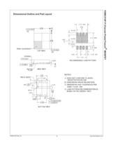
FDMC510P Rev.C5 6 www.fairchildsemi.com FDMC510P P-Channel PowerTrench® MOSFET Dimensional Outline and Pad Layout
Open the catalog to page 6
FDMC510P P-Channel PowerTrench® MOSFET FDMC510P Rev.C5 7 www.fairchildsemi.com TRADEMARKS The following includes registered and unregistered trademarks and service marks, owned by Fairchild Semiconductor and/or its global subsidiaries, and is not intended to be an exhaustive list of all such trademarks. *Trademarks of System General Corporation, used under license by Fairchild Semiconductor. DISCLAIMER FAIRCHILD SEMICONDUCTOR RESERVES THE RIGHT TO MAKE CHANGES WITHOUT FURTHER NOTICE TO ANY PRODUCTS HEREIN TO IMPROVE RELIABILITY, FUNCTION, OR DESIGN. FAIRCHILD DOES NOT ASSUME ANY LIABILITY...
Open the catalog to page 7All Fairchild Semiconductor catalogs and technical brochures
-
 FOD8383 2.5 A Output Current
18 Pages
-
 Logic SELECTION GUIDE
12 Pages
-
 Automotive Solutions Guide
8 Pages
-
 Motor Drive Solution Guide
20 Pages
-
 Mobile Solutions Guide
40 Pages
-
 AUTOMOTIVE SOLUTIONS
16 Pages
-
 Power Solutions Guide
60 Pages
-
 STANDARD PRODUCTS GUIDE
72 Pages


Archived catalogs
-
 3:1 Analog Switch Products
2 Pages
-
 USB Multimedia Switches
2 Pages
-
 Analog switch & interface
12 Pages
-
 Mobile overview
4 Pages
-
 TinyLogic® Product Overview
4 Pages
-
 Optocoupler Solutions
24 Pages
-
 Motor DRIVE solutions
32 Pages
-
 LED LIGHTING SOLUTIONS
16 Pages
-
 DIGITAL DISPLAY SOLUTIONS
36 Pages
-
 RENEWABLE ENERGY SOLUTIONS
32 Pages
-
 FGPF4536 360V, PDP IGBT
8 Pages
-
 FSAR001B AC-DC Linear Regulator
12 Pages
-
 Fairchild - Power solutions
52 Pages