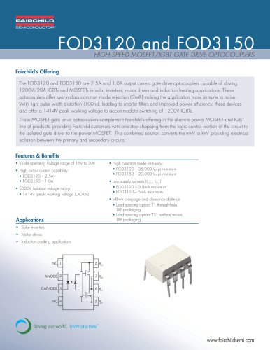
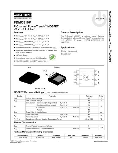
DC-DC Buck Converter Extra Small High-Performance DrMOS Package Generation III XS TM DrMOS Portfolio
2Pages

Catalog excerpts

Generation III XSTM DrMOS Portfolio Fairchild Solution Delivers the Highest Efficiency in the Industry The new DrMOS delivers 3% more efficiency than the Generation II DrMOS. And, because it’s designed for high switching frequency, engineers can reduce the output capacitors and the size of inductor to minimize the PCB space, lower the BOM cost and increase the power density. Additionally, Generation III is compatible to any analog and digital PWM controller in the industry. Features • 100% compliant to Intel DrMOS v4.0 specifications ® • Supports 5 V and 3.3 V Tri-state PWM input • 150°C thermal warning protection feature • 93% at peak and 91% at 30A, 500 KHz Freq. 12 VIN, 1 VOUT • 90% at peak and 88% at 30A, 1 MHz Freq. 12 VIN, 1 VOUT • Saving more than 50% PCB space compare to discrete solutions • High current handling: 60A at 100°C TJ • PQFN 6 mm x 6 mm chip packaging reduces VCC-to-GND and VIN-to-GND loop inductance • Helps designers to remove the heat sink • Implemented 30 K shunt resistor between gate-source, prevents C x dv/dt turn-on of the MOSFET during VIN charging • PowerTrench® with Shielded Gate Technology reduces power losses an delimates the need for a snubber circuit DC-DC Buck Converter • Capable of operating up to 1.5 MHz switching frequency Applications • High current DC-DC synchronous Buck converters • High performance servers and workstations • Telecom and networking DC-DC modules • High-end notebook PC and game consoles Extra
Open the catalog to page 1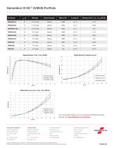
Generation III XSTM DrMOS Portfolio Part Number Module Power(V) vs IOUT, 12 VIN, 1 VOUT12 VINKHz OUT, 500 KHz VIN Range Loss Efficiency at 30 A, , 500 , 1 V Thermal Protection Module Efficiency, 12 VIN, 1 VOUT, 500 KHz 96 Module Maximum Temperature vs IOUT Module Efficiency, 12 VIN, 1 VOUT, 500 KHz Module Power Loss vs IOUT, 12 VIN, 1 VOUT, 500 KHz 8 Module Power Loss vs IOUT, 12 VIN, 1 VOUT, 500 KHz 8 7 For more information on the complete DrMOS portfolio, please visit fairchildsemi.com/drmos Silicon Valley Headquarters Module Maximum Temperature vs IOUT Corporate Offices Fairchild...
Open the catalog to page 2All Fairchild Semiconductor catalogs and technical brochures
-
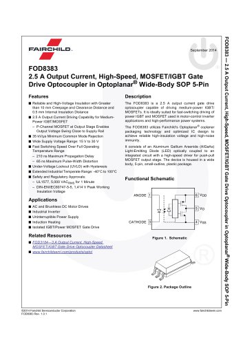
 FOD8383 2.5 A Output Current
18 Pages
-
 Logic SELECTION GUIDE
12 Pages
-
 Automotive Solutions Guide
8 Pages
-
 Motor Drive Solution Guide
20 Pages
-
 Mobile Solutions Guide
40 Pages
-
 AUTOMOTIVE SOLUTIONS
16 Pages
-
 Power Solutions Guide
60 Pages
-
 STANDARD PRODUCTS GUIDE
72 Pages


Archived catalogs
-
 3:1 Analog Switch Products
2 Pages
-
 USB Multimedia Switches
2 Pages
-
 Analog switch & interface
12 Pages
-
 Mobile overview
4 Pages
-
 TinyLogic® Product Overview
4 Pages
-
 Optocoupler Solutions
24 Pages
-
 Motor DRIVE solutions
32 Pages
-
 LED LIGHTING SOLUTIONS
16 Pages
-
 DIGITAL DISPLAY SOLUTIONS
36 Pages
-
 RENEWABLE ENERGY SOLUTIONS
32 Pages
-
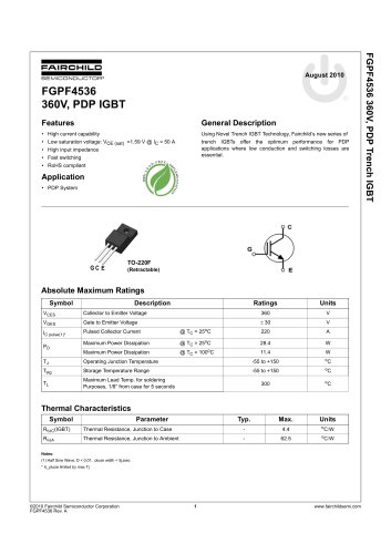 FGPF4536 360V, PDP IGBT
8 Pages
-
 FSAR001B AC-DC Linear Regulator
12 Pages
-
 Fairchild - Power solutions
52 Pages