- Catalogs
- e2v scientific instruments
- EV12AS350A
EV12AS350A
1 /90Pages

EV12AS350A
1 /90Pages
Catalog excerpts

12-bit 5.4Gsps Analog to Digital Converter ■ Dual tone dynamic performance: Applications ■ High Speed Data Acquisition ■ Direct RF Down conversion ■ Ultra Wideband Satellite Digital Receiver ■ 16 Gbps pt-pt microwave receivers ■ High energy Physics ■ Automatic Test Equipment ■ High Speed Test Instrumentation ■ LiDAR (Light Detection And Ranging) ■ Software Design Radio Performance improvement IP ADX4 is an IP-core for time-interleaved ADC mismatch error correction. In time-interleaved operating mode, ADX4 increases SFDR by wideband suppression of time-interleaving aliasing spurs due to ADC mismatch beyond 70 dBFS. ADX4 is available for evaluation on EV12AS350-ADX4-EVM evaluation board and can be licensed for production use. It is available for implementation on a wide range of FPGAs and with standard-cell design for ASICs. ADX4 IP can be activated on all parts having the ADX4 suffix in their part number. In addition, another IP designed specifically to improve the coding error rate of EV12AS350 is also available. The EV12AS350-ADX4-EVM evaluation module pre-loaded with these IP-cores is available for fast performance evaluation. Figure 1. ADX4 IP-core used with EV12AS350A Whilst Teledyne e2v Semiconductors SAS has taken care to ensure the accuracy of the information contained herein it accepts no responsibility for the consequences of any use thereof and also reserves the right to change the specification of goods without notice. Teledyne e2v Semiconductors SAS accepts no liability beyond the set out in its standard conditions of sale in respect of infringement of third party patents arising from the use of the devices in accordance with information contained herein. Teledyne e2v Semiconductors SAS, avenue de Rochepleine 38120 Saint-Egreve, France Holding Company: Teledyne e2v Semiconductors SAS Telephone: +33 (0)4 76 58 30 00 Contact Teledyne e2v by e-mail: [email protected] or visit www.teledvne-e2v.com for global sales and operations centers. 1 1160I- April 2018 Teledyne e2v Semiconductors SAS 2018 Teledyne e2v reserves the right to change or modify specifications and features
Open the catalog to page 1
EV12AS350A 1 Block Diagram Figure 2. Simplified Block Diagram 2 Description The ADC is made up of four identical 12-bit ADC cores where all four ADCs are all interleaved together. All four ADCs are clocked by the same external input clock signal delayed with the appropriate phase. The Clock Circuit is common to all four ADCs. This block receives an external 5.4 GHz clock (maximum frequency) and preferably a low jitter sinewave signal. In this block, the external clock signal is then divided by FOUR in order to generate the internal sampling clocks: The in-phase 1.35 GHz clock is sent to ADC A...
Open the catalog to page 2
Notes: 1. For simplification purpose of the timer circuit, the temporary order of ports for sampling is A C B D, therefore sampling order at output port is as follows: A: N N + 4, N + 8, . . The T/H (Track and Hold) is located after the internal 100 ohms impedance and before the ADC cores. This block is used to track the data when the internal sampling clock is low and to hold the data when the internal sampling clock is high. The ADC cores are identical for the four ADCs and each can be powered ON or DOWN individually. Each one includes a quantifier block as well as a fast logic block...
Open the catalog to page 3
Notes: TJ refers to the junction temperature at the hot spot (refer to Figure 28 for diode temperature measurement). 1160I- April 2018 Teledyne e2v Semiconductors SAS 2018 Teledyne e2v reserves the right to change or modify specifications and features without notice at any time
Open the catalog to page 4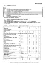
1160I- April 2018 Teledyne e2v Semiconductors SAS 2018 Teledyne e2v reserves the right to change or modify specifications and features without notice at any time
Open the catalog to page 5
1. Maximum currents are obtained with maximum supplies and maximum temperature 2. Maximum number of power-up is limited by the maximum number of OTP reading. 3. The DC analog common mode voltage is provided by ADC. CMIRef can be adjusted thanks to SPI. 1160I- April 2018 Teledyne e2v Semiconductors SAS 2018 Teledyne e2v reserves the right to change or modify specifications and features without notice at any time
Open the catalog to page 6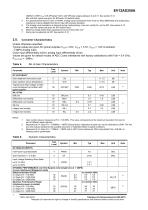
CMIRef= 0.656*VccA+(16-SPIcode)*12mV with SPIcode ranging between 0 and 31. See section 5.14 Min and Max values are given for SPIcode=16 (default value) 4. For optimal performance in term of VSWR, analog input transmission lines must be 100Q differential and analog input resistance must be digitally trimmed to cope with process deviation. 5. The Analog input impedance is trimmed during manfucaturing. User can modify RIN via the SPI. See section 5.13. Min and Max values are given for SPI default value. 6. Maximum single ended load capacitance has to be less than 5 pF 7. Swing can be adjusted via...
Open the catalog to page 7
1160I- April 2018 Teledyne e2v Semiconductors SAS 2018 Teledyne e2v reserves the right to change or modify specifications and features without notice at any time
Open the catalog to page 8
1160I- April 2018 Teledyne e2v Semiconductors SAS 2018 Teledyne e2v reserves the right to change or modify specifications and features without notice at any time
Open the catalog to page 9
1. See definition of terms in section 3.8. 2. Theoretical gain due to averaging is +1 bit on ENOB and +6dB on SNR. However, as 4 ADC cores are not perfectly matched, the actual gain is lower. 3. Performance enhancement of EV12AS350 with ADX4 is active from DC up to 2300 MHz. 4. TILD may be subject to variation over the ADC life time and environment conditions. It could potentially affect ENOB, SFDR and SInAd. To keep the same level of performance, the Offset, Gain and Phase adjustments of the ADC cores can be recalibrated as described in section 5.8.5. An other option is to use ADX4 IP. 3.6....
Open the catalog to page 10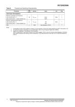
Table 6. Transient and Switching Characteristics 1. Functionality CLOCK_DIV2 enables to divide by 2 in the frequency of the clock signal applied to the ADC. See section 5.10. 2. For optimum dynamic performance, it is recommended to have a clock frequency higher than 500MHz 3. Output error amplitude > 128 LSB (3% of the full-scale). CeR is independent of input signal frequency and power supplies. CER is improved reducing clock frequency, increasing input signal amplitude and reducing junction temperature. CER performance are improved on EV12AS350B (Addendum 1201A). 1160I- April 2018 Teledyne...
Open the catalog to page 11All E2v scientific instruments catalogs and technical brochures
 Emerald 8M/12M/16M
2 Pages
 Snappy 2M
2 Pages
 EV12AD550B
49 Pages
 EV12AD550
49 Pages
 EV12AD500A
48 Pages
 EV12AQ600
57 Pages
 VEGA™ - CIS113
28 Pages
 DiViiNA® LM1
8 Pages
 ELiiXA+ 16k mono and colour
2 Pages
 CCTWTs N10503
4 Pages
 ELiiXA® 4S
2 Pages
 ELiiXA+ 8k/4k pixels
2 Pages
 AT84AD001B Dual 8-bit 1 Gsps ADC
68 Pages
 Compact modulator
2 Pages
 MP-7217 & VQ548MP
4 Pages
 High-power pulsed thyratrons
2 Pages
 Imaging brochure
11 Pages
 AViiVA® UM8
2 Pages
 AViiVA® UM4
2 Pages
 AViiVA® UM2
2 Pages
 AViiVA® UC2
2 Pages
 AViiVA® SM2
2 Pages
 AViiVA® SC2
2 Pages
 AViiVA® EM4
2 Pages
 AViiVA® EM2
2 Pages
 AViiVA® EM1
2 Pages
 StellarMini?
4 Pages
 ELiiXA® UC4/UC8
2 Pages
 ELiiXA® 3V
2 Pages
 DiViiNA® LM2
2 Pages
 EV76C454
2 Pages
 Inductive output tubes
2 Pages


- Visible imager
- CMOS camera module
- Full-color camera system
- Image processing camera module
- Monochrome camera module
- Generator
- GigE Vision camera
- Signal amplifying integrated circuit
- Compact imager
- HD camera module
- Transceiver module
- High-speed camera module
- CCD video camera
- High-performance imager
- Smart camera
- Machine vision video camera
- Spark optical emission camera module
- High-sensitivity video camera
- Processor
- Radio transceiver module