
- Catalogs
- e2v scientific instruments
- EV12AQ600

EV12AQ600

EV12AQ600
Catalog excerpts

EV12AQ600 Quad 12bit 1.5 Gsps ADC with embedded cross-point switch, Digitizing up to 6 GSps Datasheet 1203 OVERVIEW EV12AQ600 is a quad channel 12-bit 1.5 GSps ADC. The built-in Cross-Point-Switch (CPS) allows multimode operation with the capability to interleave the four independent cores in order to reach higher sampling rates. In 4-channel operating mode, the four cores can sample, in phase, four independent inputs at 1.5 GSps. In 2-channel operating mode, the cores are interleaved by 2 in order to reach 3 GSps sampling rate on each of two inputs. In 1-channel operating mode, a single input is propagated to each of the four cores which are interleaved by 4 in order to reach a sampling rate of 6 GSps. This high flexibility enables digitization of IF and RF signals with up to 3 GHz of instantaneous bandwidth. With an extended input bandwidth above 6 GHz (EFPBW) the EV12AQ600 allows sampling of signals directly in the C-band (4-8 GHz) without the need to translate the signal to baseband through a down-conversion stage. The ADC includes a multiple ADC chained synchronization feature to enable design of multichannel systems found in phased-array or MIMO applications. The EV12AQ600 enables the qualification of a single component which is capable of meeting a wide variety of application needs from single to multi-channel, from baseband to more than 6 GHz of input bandwidth. The latency is 126 system clock cycles. The device is built in a non-hermetic flip-chip package using HiTCE glass ceramic material in order to reach optimized RF performance and higher pin density. This circuit is designed, manufactured and will be qualified to be compliant with ESCC (European Space Components Coordination) and QML-Y space requirements. PERFORMANCE Single core performance 4 channel mode at 1.5Gsps at -1dBFS output level: - Fin = 748 MHz (NZ1): ENOB: 8.7 bit / SFDR: 71 dBFS using normal bandwidth (NFPBW) - Fin = 1480 MHz (NZ2): ENOB: 8.4 bit / SFDR: 63 dBFS (NFPBW) - Fin = 1900 MHz (NZ3): ENOB: 8.1 bit / SFDR: 64 dBFS (NFPBW) At -8 dBFS output level: - Fin = 2980 MHz (NZ4): ENOB: 8.3 bit / SFDR: 66 dBFS (EFPBW) - Fin = 3730 MHz (NZ5): ENOB: 8.2 bit / SFDR: 67 dBFS (EFPBW) - Fin = 5300 MHz (NZ5): ENOB: 8.1 bit / SFDR: 64 dBFS (EFPBW) SFDR@-8dBFS is better than 60 dBFS up to the 8th Nyquist and ENOB is better than 7.9 bit. Broadband performance at -14dB loading factor: 4 channel mode at 1.5 GSps over 600MHz bandwidth - NPR = 44 dB in 1st Nyquist (NFPBW) - NPR = 43.5 dB in 2nd Nyquist (NFPBW) - NPR = 43 dB in 3rd Nyquist (EFPBW) - NPR = 42.5 dB in 4th Nyquist (EFPBW) 1 channel mode at 6 GSps over 2400MHz bandwidth - NPR = 42 dB in 1st Nyquist (NFPBW) - NPR = 40 dB in 2nd Nyquist (EFPBW) SFDR in 4 channel mode without H2 and H3 harmonics is better than 70 dBFS at -1 dBFS up to 5980MHz. The 0.5 dB Gain Flatness in extended bandwidth is typically 4GHz. FEATURES 1 Vpp 100Q differential DC/AC coupled input voltage 100Q Differential input AC coupled clock Cross-point switch enabling 1, 2 or 4 channel mode at 6 GSps/3 GSps/1.5 GSps 4.5/6GHz selectable analog input bandwidth (-3dB) Low Latency ESIstream serial link at 12 Gbps Power supply: 3.3V (analog), 2.5V (I/O), 1.2V (digital), optional 1.8V (SPI) Power consumption: 6.6W SPI digital interface (gain, offset, sampling delay adjust, test modes) One time programmable anti-fuses for calibration settings ADC Gain, Offset, Sampling delay adjustment Package: CBGA323 (HiTCE) 16x16mm pitch 0.80mm Clock and SYNC chaining Extended temperature range: Tc -55°C / Tj +125°C Whilst Teledyne e2v Semiconductors SAS has taken care to ensure the accuracy of the information contained herein it accepts no responsibility for the consequences of any use thereof and also reserves the right to change the specification of goods without notice. Teledyne e2v Semiconductors SAS accepts no liability beyond the set out in its standard conditions of sale in respect of infringement of third party patents arising from the use of the devices in accordance with information contained herein. Teledyne e2v Semiconductors SAS, avenue de Rochepleine 38120 Saint-Egreve, FranceHolding Company: Teledyne e2v Semiconductors SAS Telephone: +33 (0)4 76 58 30 00 Contact Teledyne e2v by e-mail: [email protected] or visit www.teledyne-e2v.com for global sales and operations centres.
Open the catalog to page 1
EV12AQ600 INTRODUCTION This document is the Preliminary Datasheet of 12-bit 4x1.5GSps ADC with embedded Cross Point Switch (P/N EV12AQ600) Document subject to disclaimer on page 1 page 2
Open the catalog to page 2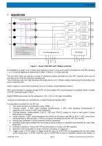
Figure 1 - Quad 12-bit ADC with 12Gbps serial link EV12AQ600 is a quad 12 bit 1.5Gbps ADC featuring a built in cross-point switch (controlled thru the SPI) allowing 1, 2 or 4 channel digitizing at respectively 6 GSps, 3 GSps or 1.5 GSps data rate. The four ADC cores can operate in phase or interleaved (option controlled thru the SPI). External clock must be provided at four times the individual sampling rate. The architecture uses four high sampling rate single cores (up to 1.5GSps) without interleaving thus providing high level of spectral purity. Data is output on a short latency serial link...
Open the catalog to page 3
the ADC, SYNCO is a synchronized copy of SYNCTRIG, for the serial link version PRBS are reset by a SYNC pulse). • Swing Adjust: Output swing of both serial links and timer CML or LVDS buffers is reduced by 30% for power dissipation reduction purpose. • Output buffer impedance adjust (trim by a range of 20%) to improve transmission • 12 Gbps Serial link polarity can be inverted The ADC features internal DACs controlled thru the SPI for tuning: • Sampling Delay Adjust 12 bit with 120ps tuning range : o 2 bit for coarse step (~ 30ps/step) o 10 bit for fine step (~ 30fs/step) • Gain Adjust: 4096...
Open the catalog to page 4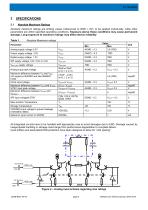
2 SPECIFICATIONS 2.1 Absolute Maximum Ratings Absolute maximum ratings are limiting values (referenced to GND = 0V), to be applied individually, while other parameters are within specified operating conditions. Exposure above those conditions may cause permanent damage. Long exposure to maximum ratings may affect device reliability Table 1._Absolute Maximum ratings All integrated circuits have to be handled with appropriate care to avoid damages due to ESD. Damage caused by inappropriate handling or storage could range from performance degradation to complete failure. Input buffers and associated...
Open the catalog to page 5All E2v scientific instruments catalogs and technical brochures
 Emerald 8M/12M/16M
2 Pages
 Snappy 2M
2 Pages
 EV12AS350A
90 Pages
 EV12AD550B
49 Pages
 EV12AD550
49 Pages
 EV12AD500A
48 Pages
 VEGA™ - CIS113
28 Pages
 DiViiNA® LM1
8 Pages
 ELiiXA+ 16k mono and colour
2 Pages
 CCTWTs N10503
4 Pages
 ELiiXA® 4S
2 Pages
 ELiiXA+ 8k/4k pixels
2 Pages
 AT84AD001B Dual 8-bit 1 Gsps ADC
68 Pages
 Compact modulator
2 Pages
 MP-7217 & VQ548MP
4 Pages
 High-power pulsed thyratrons
2 Pages
 Imaging brochure
11 Pages
 AViiVA® UM8
2 Pages
 AViiVA® UM4
2 Pages
 AViiVA® UM2
2 Pages
 AViiVA® UC2
2 Pages
 AViiVA® SM2
2 Pages
 AViiVA® SC2
2 Pages
 AViiVA® EM4
2 Pages
 AViiVA® EM2
2 Pages
 AViiVA® EM1
2 Pages
 StellarMini?
4 Pages
 ELiiXA® UC4/UC8
2 Pages
 ELiiXA® 3V
2 Pages
 DiViiNA® LM2
2 Pages
 EV76C454
2 Pages
 Inductive output tubes
2 Pages


- Visible imager
- CMOS camera module
- Full-color camera system
- Monochrome camera module
- Image processing camera module
- GigE Vision camera
- Compact imager
- HD camera module
- Signal amplifying integrated circuit
- Generator
- Transceiver module
- High-speed camera module
- CCD video camera
- High-performance imager
- Smart camera
- Spark optical emission camera module
- Machine vision video camera
- High-sensitivity video camera
- Processor
- Camera Link video camera