
- Catalogs
- e2v scientific instruments
- EV12AD550

EV12AD550

EV12AD550
The EV12AD550 is a dual S-band capable 12-bit ADC designed for space applications, featuring a single core architecture for high spectral purity. It supports direct digitization in the S-band with a 3dB input bandwidth up to 4.3GHz, and can operate beyond 5GHz with reduced dynamic range. The device includes synchronization features for large arrays of synchronous ADCs, beneficial for applications like active antenna arrays or MIMO systems. It offers cross-talk isolation over 80dB and a Noise Power Ratio (NPR) of 50dB in the first Nyquist zone. The ADC is housed in a hermetic flip chip CCGA323 package with improved thermal performance and is planned for QML-V and ESCC certification.
- Earth observation SAR payload
- Telecommunication satellite payload
- Satellite data links
- Satellite altimeter
- Satellite TWTA compensation system
- Satellite to satellite laser data links
- Dual channel 12 bits 1.5GSps ADC
- Single core architecture per channel
- Differential analog input voltage: 1Vppd
- Full Power Input bandwidth (-3dB): 4.3GHz
- Power consumption: 2.3W per channel
- Power supplies: Single Rail 3.4V or Dual rail 3.4V/2.5V
- Low latency output interface: LVDS DEMUX 1:1 or 1:2
- SPI configuration with space protection control
- Multiple ADC chained synchronization
- Test modes: ramp, flash, PRBS
- Clock input at 3GHz
- 4.3GHz analog input bandwidth (-3dB)
- 50 dB NPR over 1st Nyquist
- 48 dB NPR over 2nd Nyquist
- 46 dB NPR over 3rd Nyquist
- 45 dB NPR over 4th Nyquist
- 74 dBFS SFDR at 100MHz, -1dBFS
- 72 dBFS SFDR at 1900MHz, -8dBFS
- 60 dBFS SFDR at 3730MHz, -12dBFS
- 49 dBFS SFDR at 5300MHz, -12dBFS
- Latency < 10ns
Absolute Maximum Ratings
These are limiting values that should not be exceeded to avoid permanent damage. Long exposure to these conditions may affect device reliability.
Specifies the optimal operating conditions for the device, including supply voltages and temperature ranges.
Details the power requirements, input and output characteristics, and other electrical parameters under typical and maximum conditions.
Explains the different levels of testing conducted to ensure device performance and reliability.
Typical values are provided for dual-rail configurations at 25°C. Minimum and maximum values depend on the test level, specified at a sampling frequency of 1.5GSps with SDA disabled and reduced swing mode.
Key parameters include gain variation, DC offset, differential non-linearity (DNL), and integral non-linearity (INL). Gain variation ranges from -1.5 to 1.5 dB, while DC offset is between 2045 and 2051 LSB. DNL and INL are specified with no missing code and a maximum deviation of 6.5 LSB.
Includes full power input bandwidth, gain flatness, and input voltage standing wave ratio (VSWR). Noise power ratio (NPR) and spurious free dynamic range (SFDR) are detailed for various Nyquist zones and input frequencies. Total harmonic distortion (THD) and signal-to-noise ratio (SNR) are also specified.
Typical values are given for dual-rail configurations at 25°C. Parameters include ADC code error rate, overvoltage recovery time, and various timing characteristics such as aperture delay and output data pipeline delay.
The ADC digital output coding table provides binary representations for differential analog input voltage levels.
Key terms such as Code Error Rate (CER), Differential Non-Linearity (DNL), Effective Number Of Bits (ENOB), and Noise Power Ratio (NPR) are defined to clarify the specifications and performance metrics.
The ADC is housed in a Hermetic Ceramic Column Grid Array (CCGA323) with a body size of 21mm x 21mm and a mass of 7g. The substrate is made of Aluminum Nitride (AlN), and the lid is Kovar polarized at AGND. The package includes 323 pins with a 1.0mm pitch.
Thermal resistance values are provided for different junctions, calculated using thermal simulation methods. The document notes that thermal paths to the top of the lid and bottom of columns should be considered in a three-resistor model for accurate thermal management.
Detailed pinout information is provided, including descriptions and simplified electrical schematics for power supplies, clock signals, analog inputs, digital outputs, and SPI digital I/O. The pinout table specifies the function and electrical characteristics of each pin.
The document outlines the functional description of various components, including power supplies, analog inputs, clock inputs, and digital outputs. It also describes the digital reset and startup procedure, emphasizing the importance of the RSTN signal for initializing the device.
The document advises on the use of an asynchronous active low global reset (RSTN) during power-up to ensure proper initialization of SPI and OTP registers. It also provides guidelines for using the SPI interface and managing thermal paths effectively.
- Using the SPI Interface: The device requires a reset at power-up through RSTN, which is active low and must last at least 10µs. During this pulse, CSN must be high and SCLK low. The clock (CLK) should be provided before the RSTN pulse. After a 1ms delay, the SPI instruction WRITE @0x7E 0x0001 is sent to the ADC to load OTP into SPI registers. The ADC is then configured via the SPI interface, and a pulse on the SYNCTRIG input resets internal clocks. The ADC can be set to trigger mode, and the SE_protect register can be activated.
- Without Using the SPI Interface: The device also requires a reset at power-up through RSTN, with CSN and SCLK held high. The CLK must be provided before the RSTN pulse. A pulse on the SYNCTRIG input resets internal clocks, after which normal ADC operation can commence.
- The SPI interface uses RSTN, SCLK, CSN, MISO, and MOSI signals. It follows a standard SPI protocol with 8 address bits and 16 data bits. The MOSI sequence starts with '0' for read and '1' for write procedures.
- Registers are mapped with specific addresses and default values, allowing for various configurations such as bandwidth selection, input impedance trimming, and swing adjustments.
- The ADC output can be configured as DEMUX 1:1 or 1:2 through the SPI register OUT_SEL. Power supply configurations vary based on the selected output mode.
- Control bits XFU1 and XFU2 can output in-range, parity, or trigger signals, configurable through the CTRL_BIT_CFG register.
- Input impedance can be trimmed to 100Ω with a precision of +/-2.4Ω. The input bandwidth is selectable through the CHIP_CTRL register, with nominal and extended bandwidth options.
- Input common mode can be trimmed to optimize linearity performance, with a range of 340mV available through 32 steps.
- The selection between SYNC and TRIGGER modes is controlled by bit 7 of the SPI register CHIP_CTRL. SYNC mode is the default.
SYNC mode is essential for deterministic timing in core synchronization and ADC alignment. A SYNC pulse is required post power-up to reset clock dividers and test modes. The SYNC signal must align with the external clock and adhere to specified timing. The SYNCTRIG input can be configured via the SYNC_CTRL register, with edge recovery options controlled by the ESEL bit.
In trigger mode, the SYNCTRIG input is mirrored on the XFUn pin with a pipeline delay matching the sampled data. This mode is detailed further in the Control bit XFU1 and XFU2 section.
SYNCO is a resampled version of SYNCTRIG, useful for device synchronization. SSO is a clock signal divided by 16 from the master clock, providing a reference for synchronization. Both outputs are LVDS signals with configurable swing via the CHIP_CTRL register.
Factory calibration includes two sets for different temperatures, selectable via the CHIP_CTRL register. Calibration loading requires writing to the LOAD_CAL register.
Two test modes, flash and ramp, are available for interface validation. These are enabled through the TEST_MODE register. Ramp mode outputs a 12-bit ramp, while flash mode aids in FPGA-ADC alignment.
Extra protection is available via the EXTRA_SEE_PROTECT register, which disables SYNCTRIG input in SYNC mode to prevent unwanted resets.
Calibration verification is possible through CRC checks, with reference values stored in OTP registers. Successful loading is confirmed when calculated and reference CRC values match.
Sampling clocks can be interleaved or aligned, controlled by the CLKINT bit in the CHIP_CTRL register. Calibration for offset, gain, and phase is available through specific registers, with adjustments made via embedded DACs.
SDA allows independent adjustment of ADC core sampling instants, providing a 10ps tuning range. It must be enabled on both channels for proper operation.
Channels can enter stand-by independently, reducing power consumption while maintaining output interface functionality.
A diode allows temperature monitoring, with voltage readings indicating junction temperature.
Bandwidth, crosstalk, and performance metrics like SFDR, THD, ENOB, SINAD, and SNR are characterized, with graphs illustrating performance across input frequencies.
The ADC can operate with a single rail, and it is recommended to use ferrite and decoupling capacitance to prevent power supply pollution. Specific decoupling capacitor configurations are provided for different DEMUX modes.
The analog inputs can be DC or AC coupled. Phase and amplitude imbalances affect linearity, so input drivers should minimize these effects, and trace lengths should be matched.
The document lists various models of the ADC, including prototypes, engineering models, and flight models, with details on package type, temperature range, and screening levels.
The document includes a revision history detailing updates and corrections made in various versions, including changes to performance metrics, pinout clarifications, and the addition of production part numbers.
Recommendations for power supply configurations and analog input handling are provided to optimize ADC performance. The document also includes detailed tables and figures illustrating decoupling strategies and performance metrics.
Catalog excerpts

TELEDYNE e2VEverywhereyoulook™ EV12AD550 Dual 12bits 1.5GSps ADC Space Grade DATASHEET OVERVIEW EV12AD550 is a dual S-band capable 12bit ADC intended for space applications that is built using a true single core architecture providing high spectral purity. With a 3dB input bandwidth up to 4.3GHz it allows for direct digitization in S-band without frequency down-conversion. Synthetic Aperture Radar systems will also be able to operate this ADC with reduced dynamic range at frequencies beyond 5GHz without frequency down-conversion. This device includes a multiple ADC chained synchronization feature. This would help designing large array of synchronous ADC for example in active antenna array or MIMO systems. Multichannel applications will benefit from a cross-talk isolation between inputs in excess of 80dB and Noise Power Ratio performance of 50dB in the first Nyquist zone. This device comes in a hermetic flip chip CCGA323 package in Aluminum Nitride with improved thermal performance and is planned for QML-V and ESCC certification. APPLICATIONS ■ Earth observation SAR payload ■ Telecommunication satellite payload ■ Satellite data links ■ Satellite altimeter ■ Satellite TWTA compensation system ■ Satellite to satellite laser data links FEATURES Dual channel 12 bits 1.5GSps ADC ■ Single core architecture ADC per channel ■ Differential analog input voltage: 1Vppd ■ Full Power Input bandwidth (-3dB): 4.3GHz ■ Differential clock input ■ Power consumption: 2.3W / channel ■ Power supplies: Single Rail 3.4V or Dual rail 3.4V/2.5V ■ Low latency output interface: LVDS DEMUX 1:1 or 1:2 ■ Package: Hermetic CCGA323 21x21mm / 1mm pitch, Aluminum nitride material ■ SPI configuration with space protection control ■ Multiple ADC chained synchronization ■ Test mode: ramp, flash, PRBS ■ Control bit: parity, in-range, trigger ■ Clock input at 3GHz PERFORMANCE @ 1.5GSps 4.3GHz analog input bandwidth (-3dB) 50 dB NPR over 1st Nyquist 48 dB NPR over 2nd Nyquist 46 dB NPR over 3rd Nyquist 45 dB NPR over 4th Nyquist 74 dBFS SFDR at 100MHz, -1dBFS 72 dBFS SFDR at 1900MHz, -8dBFS 60 dBFS SFDR at 3730MHz, -12dBFS 49 dBFS SFDR at 5300MHz, -12dBFS Latency < 10ns Whilst Teledyne e2v has taken care to ensure the accuracy of the information contained herein it accepts no responsibility for the consequences of any use thereof and also reserves the right to change the specification of goods without notice. Teledyne e2v accepts no liability beyond the set out in its standard conditions of sale in respect of infringement of third party patents arising from the use of tubes or other devices in accordance with information contained herein. Teledyne e2v Semiconductors SAS, Avenue de Rochepleine, BP 123, 38521 Saint Egreve Cedex France Telephone: +33 (0)476 58 30 00 Facsimile: +33 (0)4 76 58 34 80. Contact Teledyne e2v by e-mail:HOTLINE : [email protected] for technical purpose and [email protected] for commercial information. Visit www.teledyne-e2v.com for global sales and operations centres © Teledyne e2v Semiconductors SAS 2017 DS-1
Open the catalog to page 1
Dual channel 12 bits 1.5GSps ADC1 Block Diagrams 1.1 DEMUX 1:1 SYNC/TRIGG 1.2 DEMUX 1:2 ADR Channel A data ready High port BDR Channel B data ready High port Document subject to disclaimer on page 1
Open the catalog to page 2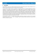
Dual channel 12 bits 1.5GSps ADC The EV12AD550 is a dual 12 bit 1.5GSps ADC featuring low latency LVDS parallel output with a built-in selectable 1:2 or 1:1 DEMUX to compromise between power consumption and ease of interfacing. The two channels can operate in phase or in opposition, thus allowing synchronous or interleaved sampling. Each channel is composed of a true single core ADC sampling at up to 1.5GSps. Based on an innovative architecture without internal interleaving, it provides high spectral purity. It offers an analog input bandwidth of up to 4.3GHz with 2 selectable configurations...
Open the catalog to page 3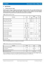
Dual channel 12 bits 1.5GSps ADC 3 Specifications 3.1 Absolute maximum ratings Absolute maximum ratings are limiting and stressing values (referenced to GND = 0V), to be applied individually, while other parameters are within specified operating conditions. Exposure above those conditions may cause permament damage. Long exposure to maximum ratings may affect device reliability. Functional operation at any other conditions those indicated in the operational section may affect devices performances and reliability. Table 1: Absolute maximum ratings Document subject to disclaimer on page 1
Open the catalog to page 4
Dual channel 12 bits 1.5GSps ADC3.2 Recommended conditions of use Table 3: Recommended conditions of use Only MIN and MAX values are guaranteed Document subject to disclaimer on page 1
Open the catalog to page 5
Dual channel 12 bits 1.5GSps ADC 3.4 Electrical characteristics for supplies, inputs and outputs Unless otherwise specified: - Typical values are given for typical supplies in single-rail configuration (Refer to Table 18 in section DEMUX 1:1 or 1:2 for more information) at Tamb = +25°C. - Minimum and maximum values are given over corresponding temperature range for typical power supplies. - Values are given with SDA disabled and reduced swing mode - Sampling frequency (Fs ) at 1.5Gsps Table 6: Electrical characteristics for supplies, inputs and outputs Parameter Test level Symbol Min Value Unit...
Open the catalog to page 6
Dual channel 12 bits 1.5GSps ADC Parameter Document subject to disclaimer on page 1
Open the catalog to page 7
Dual channel 12 bits 1.5GSps ADC Parameter Notes: 1. Refer to Table 18 in section DEMUX 1:1 or 1:2 for more information on power supplies management 2. Enabling SDA increases power consumption by 80mW (23mA on VCCA) 3. The DC analog common mode voltage is provided by the CMIREF output of the ADC 4. See section Input common mode trimming for more information on the range available. 5. For optimal performance, in terms of VSWR, the input impedance must be 100Q ± 5% and the analog input impedance must be digitally trimmed to cope with process deviation. Refer to section Input impedance trimming...
Open the catalog to page 8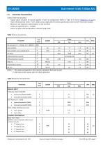
Dual channel 12 bits 1.5GSps ADC 3.5 Converter characteristics Unless otherwise specified: - Typical values are given for typical supplies in dual-rail configuration (Refer to Table 18 in section DEMUX 1:1 or 1:2 for more information) at Tamb = +25°C. Both cores comply with the below specification when the OTP have been loaded. - Minimum and maximum values depend on the test level. - Values are specified at Fs = 1.5GSps. - Values are given with SDA disabled, reduced swing mode. Table 7: Static characteristics Document subject to disclaimer on page 1
Open the catalog to page 9All E2v scientific instruments catalogs and technical brochures
 Emerald 8M/12M/16M
2 Pages
 Snappy 2M
2 Pages
 EV12AS350A
90 Pages
 EV12AD550B
49 Pages
 EV12AD500A
48 Pages
 EV12AQ600
57 Pages
 VEGA™ - CIS113
28 Pages
 DiViiNA® LM1
8 Pages
 ELiiXA+ 16k mono and colour
2 Pages
 CCTWTs N10503
4 Pages
 ELiiXA® 4S
2 Pages
 ELiiXA+ 8k/4k pixels
2 Pages
 AT84AD001B Dual 8-bit 1 Gsps ADC
68 Pages
 Compact modulator
2 Pages
 MP-7217 & VQ548MP
4 Pages
 High-power pulsed thyratrons
2 Pages
 Imaging brochure
11 Pages
 AViiVA® UM8
2 Pages
 AViiVA® UM4
2 Pages
 AViiVA® UM2
2 Pages
 AViiVA® UC2
2 Pages
 AViiVA® SM2
2 Pages
 AViiVA® SC2
2 Pages
 AViiVA® EM4
2 Pages
 AViiVA® EM2
2 Pages
 AViiVA® EM1
2 Pages
 StellarMini?
4 Pages
 ELiiXA® UC4/UC8
2 Pages
 ELiiXA® 3V
2 Pages
 DiViiNA® LM2
2 Pages
 EV76C454
2 Pages
 Inductive output tubes
2 Pages


- Visible imager
- CMOS camera module
- Full-color camera system
- Monochrome camera module
- Image processing camera module
- GigE Vision camera
- Compact imager
- HD camera module
- Signal amplifying integrated circuit
- Generator
- Transceiver module
- High-speed camera module
- CCD video camera
- High-performance imager
- Smart camera
- Spark optical emission camera module
- Machine vision video camera
- High-sensitivity video camera
- Processor
- Camera Link video camera