
- Catalogs
- e2v scientific instruments
- EV12AD500A

EV12AD500A

EV12AD500A
Catalog excerpts

Bringing life \ ^ ^ V to technology PRELIMINARY DATASHEET OVERVIEW EV12AD500A is a dual S-band capable 12bit ADC intended for various applications that is built using a true single core architecture providing high spectral purity. With a 3dB input bandwidth of 5.2GHz it allows for digitization in S-band without frequency conversion. Wideband communication and radar systems will also be able to operate this ADC with reduced dynamic range at frequencies beyond 5GHz without frequency down-conversion. This device outputs data either in LVDS format with low latency or high speed serial link using the ESIstream (Efficient Serial Interface) protocol. It proposes a multiple ADC chained synchronization feature. Along with the serial interface, it helps designing large array of synchronous ADC in active antenna array or MIMO systems. Dual channel crosstalk isolation exhibits figure in excess of 80dB and Noise Power Ratio performance beyond 50dB in the first Nyquist zone. This device comes in a flip chip CBGA255 package in HiTCE® substrate with High Temperature Coefficient of Expansion. APPLICATIONS ■ Wideband communication system ■ Phased-array/MIMO communication system ■ Phased-array/MIMO radar system ■ Instrumentation FEATURES Dual channel 12 bits 1.5GSps ADC ■ Single core architecture ADC ■ Differential analog input voltage: 1Vppd ■ Full Power Input bandwidth (-3dB): 5.2GHz ■ Differential clock input ■ Power consumption: 2.3W / channel ■ Power supplies: Single Rail 3.4V or Dual rail 3.4V/2.5V ■ Output interface: LVDS DEMUX 1:1 or serial ESIstream ■ Package: CBGA255 14x14mm / 0.8mm pitch ■ SPI configuration ■ Multiple ADC chained synchronization ■ Test mode: ramp, flash, PRBS ■ Control bit: parity, in-range, trigger, timestamp ■ Clock input up to 3GHz PERFORMANCE @ 1.5GSps ■ 5.2GHz analog input bandwidth (-3dB) ■ 50 dB NPR over 1st Nyquist ■ Latency < 7.5ns in LVDS output ■ Latency < 17ns in serial output Whilst e2v technologies has taken care to ensure the accuracy of the information contained herein it accepts no responsibility for the consequences of any use thereof and also reserves the right to change the specification of goods without notice. e2v technologies accepts no liability beyond the set out in its standard conditions of sale in respect of infringement of third party patents arising from the use of tubes or other devices in accordance with information contained herein. e2v technologies (uk) limited, Waterhouse Lane, Chelmsford, Essex CM1 2QU United Kingdom Holding Company: e2v technologies plc Telephone: +44 (0)1245 493493 Facsimile: +44 (0)1245 492492 Contact e2v by e-mail: [email protected] or visit www.e2v.com for global sales and operations centres.
Open the catalog to page 1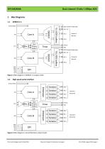
Dual channel 12 bits 1.5GSps ADC1 Bloc Diagrams 1.1 DEMUX 1:1 ADR Channel A data ready High port BDR Channel B data ready High port 1.2 High speed serial interface Document subject to disclaimer on page 1
Open the catalog to page 2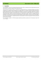
Dual channel 12 bits 1.5GSps ADC The EV12AD500A is a dual 12 bit 1.5GSps ADC featuring low latency LVDS 1:1 parallel output and a high speed serial output option based on the ESIstream (Efficient Serial Interface) protocol. The two channels can operate in phase or in opposition, thus allowing synchronous or interleaved sampling. Each channel is composed of a true single core ADC sampling at up to 1.5GSps. Based on an innovative architecture without interleaving, it provides high spectral purity. It offers an analog input bandwidth up to 5.2GHz with 2 selectable configurations to optimize SNR...
Open the catalog to page 3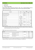
Dual channel 12 bits 1.5GSps ADC 3 Specifications 3.1 Absolute maximum ratings Absolute maximum ratings are limiting values (referenced to GND = 0V), to be applied individually, while other parameters are within specified operating conditions. Exposure to maximum ratings may affect device reliability. Table 1: Absolute maximum ratings Document subject to disclaimer on page 1
Open the catalog to page 4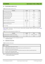
Dual channel 12 bits 1.5GSps ADC3.2 Recommended conditions of use Table 3: Recommended conditions of use Notes: Only MIN and MAX values are guaranteed. 1. Unless otherwise specified Document subject to disclaimer on page 1
Open the catalog to page 5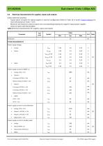
Dual channel 12 bits 1.5GSps ADC 3.4 Electrical characteristics for supplies, inputs and outputs Unless otherwise specified: - Typical values are given for typical supplies in dual-rail configuration (Refer to Table 18 in section Output selection for more information) at Tamb = +25°C - Minimum and maximum values are given over corresponding temperature range for typical power supplies - Values are given with SDA disabled Table 6: Electrical characteristics for supplies, inputs and outputs Document subject to disclaimer on page 1
Open the catalog to page 6
Document subject to disclaimer on page 1
Open the catalog to page 7
Notes: 1. Refer to Table 18 in section Output selection for more information on power supplies management 2. Enabling SDA increases power consumption by 80mW (23mA on VCCA) 3. The DC analog common mode voltage is provided by the CMIREF output of the ADC 4. See section Input common mode trimming for more information on the range available 5. For optimal performance, in terms of VSWR, the input impedance must be 50Q ± 5% and the analog input impedance must be digitally trimmed to cope with process deviation. Refer to section Input impedance trimming for more information 6. The crosstalk specified...
Open the catalog to page 8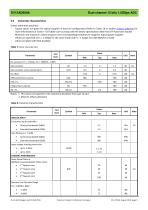
Dual channel 12 bits 1.5GSps ADC 3.5 Converter characteristics Unless otherwise specified: - Typical values are given for typical supplies in dual-rail configuration (Refer to Table 18 in section Output selection for more information) at Tamb = +25°CBoth cores comply with the below specification when the OTP have been loaded - Minimum and maximum values are given over corresponding temperature range for typical power supplies - Values are specified at Fs = 1.5GSps for the serial mode and Fs = 1.3GSps for LVDS DMUX1:1 mode - Values are given with SDA disabled Table 7: Static characteristics Document...
Open the catalog to page 9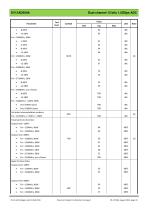
Document subject to disclaimer on page 1
Open the catalog to page 10
Dual channel 12 bits 1.5GSps ADC Parameter • Fin = 2980MHz, EBW Signal to Noise And Distortion Output level -1dBFS • Fin = 100MHz, NBW Output level -8dBFS • Fin = 100MHz, NBW • Fin = 1480MHz, NBW Effective Number Of Bits Output level -1dBFS • Fin = 100MHz, NBW • Fin = 1480MHz, NBW Output level -8dBFS • Fin = 100MHz, NBW • Fin = 1480MHz, NBW Noise Spectral density at -1dBFS • 1st Nyquist zone, NBW Noise Spectral density at -8dBFS • 1st Nyquist zone, NBW Test level dBFS dBFS dBFS dBFS dBFS dBFS dBFS dBFS dBFS dBFS dBFS dBm/Hz dBm/Hz dBm/Hz dBm/Hz dBm/Hz dBm/Hz dBm/Hz dBm/Hz...
Open the catalog to page 11All E2v scientific instruments catalogs and technical brochures
 Emerald 8M/12M/16M
2 Pages
 Snappy 2M
2 Pages
 EV12AS350A
90 Pages
 EV12AD550B
49 Pages
 EV12AD550
49 Pages
 EV12AQ600
57 Pages
 VEGA™ - CIS113
28 Pages
 DiViiNA® LM1
8 Pages
 ELiiXA+ 16k mono and colour
2 Pages
 CCTWTs N10503
4 Pages
 ELiiXA® 4S
2 Pages
 ELiiXA+ 8k/4k pixels
2 Pages
 AT84AD001B Dual 8-bit 1 Gsps ADC
68 Pages
 Compact modulator
2 Pages
 MP-7217 & VQ548MP
4 Pages
 High-power pulsed thyratrons
2 Pages
 Imaging brochure
11 Pages
 AViiVA® UM8
2 Pages
 AViiVA® UM4
2 Pages
 AViiVA® UM2
2 Pages
 AViiVA® UC2
2 Pages
 AViiVA® SM2
2 Pages
 AViiVA® SC2
2 Pages
 AViiVA® EM4
2 Pages
 AViiVA® EM2
2 Pages
 AViiVA® EM1
2 Pages
 StellarMini?
4 Pages
 ELiiXA® UC4/UC8
2 Pages
 ELiiXA® 3V
2 Pages
 DiViiNA® LM2
2 Pages
 EV76C454
2 Pages
 Inductive output tubes
2 Pages


- Visible imager
- CMOS camera module
- Full-color camera system
- Monochrome camera module
- Image processing camera module
- GigE Vision camera
- Compact imager
- HD camera module
- Signal amplifying integrated circuit
- Generator
- Transceiver module
- High-speed camera module
- CCD video camera
- High-performance imager
- Smart camera
- Spark optical emission camera module
- Machine vision video camera
- High-sensitivity video camera
- Processor
- Camera Link video camera