- Catalogs
- e2v scientific instruments
- AT84AD001B Dual 8-bit 1 Gsps ADC
AT84AD001B Dual 8-bit 1 Gsps ADC
1 /68Pages

AT84AD001B Dual 8-bit 1 Gsps ADC
1 /68Pages
Catalog excerpts

Dual ADC with 8-bit Resolution 1 Gsps Sampling Rate per Channel, 2 Gsps in Interleaved Mode Single or 1:2 Demultiplexed Output LVDS Output Format (100Ω) 500 mVpp Analog Input (Differential Only) Differential or Single-ended 50Ω PECL/LVDS Compatible Clock Inputs Power Supply: 3.3V (Analog), 3.3V (Digital), 2.25V (Output) LQFP144 or LQFP-ep 144L Green Packages Temperature Range: – 0°C < Tamb < 70° C (Commercial Grade) – –40°C < Tamb < 85° C (Industrial Grade) • 3-wire Serial Interface – 16-bit Data, 3-bit Address – 1:2 or 1:1 Output Demultiplexer Ratio Selection – Full or Partial Standby Mode – Analog Gain (± 1.5 dB) Digital Control – Input Clock Selection – Analog Input Switch Selection – Binary or Gray Logical Outputs – Synchronous Data Ready Reset – Data Ready Delay Adjustable on Both Channels – Interleaving Functions: • Offset and Gain (Channel to Channel) Calibration • Digital Fine SDA (Fine Sampling Delay Adjust) on One Channel – Internal Static or Dynamic Built-In Test (BIT) Low Power Consumption: 0.7W Per Channel Power Consumption in Standby Mode: 120 mW 1.5 GHz Full Power Input Bandwidth (–3 dB) SNR = 42 dB Typ (6.8 ENOB), THD = –51 dBc, SFDR = –54 dBc at Fs = 1 Gsps Fin = 500 MHz • 2-tone IMD3: –54 dBc (499 MHz, 501 MHz) at 1 Gsps • DNL = 0.25 LSB, INL = 0.5 LSB • Low Bit Error Rate (10–13) at 1 Gsps Visit our website: www.e2v.com for the latest version of the datasheet e2v semiconductors SAS 2009
Open the catalog to page 1
Digital Oscilloscopes Communication Receivers (I/Q) Direct RF Down Conversion High Speed Data Acquisition Radar/ECM 4. Description The AT84AD001B is a monolithic dual 8-bit analog-to-digital converter, offering low 1.4W power consumption and excellent digitizing accuracy. It integrates dual on-chip track/holds that provide an enhanced dynamic performance with a sampling rate of up to 1 Gsps and an input frequency bandwidth of over 1.5 GHz. The dual concept, the integrated demultiplexer and the easy interleaving mode make this device user-friendly for all dual channel applications, such as direct...
Open the catalog to page 2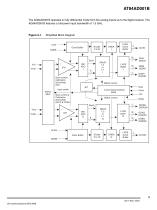
AT84AD001B The AD84AD001B operates in fully differential mode from the analog inputs up to the digital outputs. The AD84AD001B features a full-power input bandwidth of 1.5 GHz. Simplified Block Diagram Clock Buffer DDRB LVDS Clock Buffer Gain control I Calibration Gain/offset ISA I DOAI DOAIN DOBI DOBIN DMUX control Data BIT Input switch INPUT MUX Gain control Q Calibration Gain/offset ISA Q & FiSDA + S/H DMUX control DoirQ Vinq DOIRI DOIRIN DOIRQ DOIRQN DOAQ DOAQN DOBQ DOBQN CLKQ Clock Buffer DDRB LVDS Clock Buffer
Open the catalog to page 3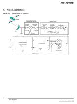
AT84AD001B 6. Typical Applications Figure 6-1. Satellite Receiver Application Low Noise Converter (Connected to the Dish) Bandpass Amplifier Satellite Tuner Low Pass Filter Bandpass Amplifier Tunable Band Filter Local oscillator Local Oscillator Control Functions: Clock Q Quadrature Demodulation
Open the catalog to page 4
Dual Channel Digital Oscilloscope Application Analog switch Channel Mode Selection Clock selection Timing circuit DACs Smart dual ADC DACs Absolute Maximum Ratings Analog positive supply voltage Digital positive supply voltage Output supply voltage Analog input voltage VINI or VINIB VINQ or VINQB Digital input voltage Clock input voltage Maximum difference between VCLK and VCLKB VCLK – VCLKB Maximum junction temperature Storage temperature Maximum difference between VCCA and VCCD Minimum VCCO Lead temperature (soldering 10s) Note: Absolute maximum ratings are limiting values (referenced to GND...
Open the catalog to page 5
Recommended Value Analog supply voltage Digital supply voltage Output supply voltage VINi – VIniB or VINQ – VINQB Differential analog input voltage (full-scale) Differential clock input level Internal Settling Adjustment (ISA) with a 3-wire serial interface for channel I and channel Q Operating temperature range Commercial grade Industrial grade 7. Electrical Operating Characteristics Unless otherwise specified: • VCCA = 3.3V; VCCD = 3.3V; VCCO = 2.25V • VINI – VINB or VINQ – VINQB = 500 mVpp full-scale differential input • LVDS digital outputs (100Ω) • Tamb (typical) = 25° C • Full temperature...
Open the catalog to page 6
Electrical Operating Characteristics in Nominal Conditions (Continued) ICCA ICCD ICCO Supply current (1 channel only, 1:2 DMUX mode) - Analog - Digital - Output ICCA ICCD ICCO Supply current (full standby mode) - Analog - Digital - Output ICCA ICCD ICCO Nominal dissipation (1 clock, 1:1 DMUX mode, 2 channels) Nominal dissipation (full standby mode) Supply current (1 channel only, 1:1 DMUX mode) - Analog - Digital - Output Analog Inputs Full-scale differential analog input voltage to obtain full scale with no gain adjust (mode 0) VINi – VIniB or – VINQB VINQ Analog input common mode Analog input...
Open the catalog to page 7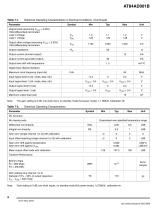
Electrical Operating Characteristics in Nominal Conditions (Continued) Output levels (assuming VCCO = 2.25V) 100Ω differentially terminated Logic 0 voltage Logic 1 voltage Output offset voltage (assuming VCCO = 2.25V) 100Ω differentially terminated Output impedance Output current (shorted output) Output current (grounded output) Output level drift with temperature Digital Input (Serial Interface) Maximum clock frequency (input clk) Input logical level 0 (clk, mode, data, ldn) Input logical level 1 (clk, mode, data, ldn) Output logical level 0 (cal) Output logical level 1 (cal) Maximum output...
Open the catalog to page 8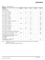
AC Performance Signal-to-noise Ratio Fs = 1 Gsps Fin = 20 MHz Fs = 1 Gsps Fin = 500 MHz Fs = 1 Gsps Fin = 1 GHz Effective Number of Bits Fs = 1 Gsps Fin = 20 MHz Fs = 1 Gsps Fin = 500 MHz Fs = 1 Gsps Fin = 1 GHz Total Harmonic Distortion (First 9 Harmonics) Fs = 1 Gsps Fin = 20 MHz Fs = 1 Gsps Fin = 500 MHz Fs = 1 Gsps Fin = 1 GHz Spurious Free Dynamic Range Fs = 1 Gsps Fin = 20 MHz Fs = 1 Gsps Fin = 500 MHz Fs = 1 Gsps Fin = 1 GHz Two-tone Inter-modulation Distortion (Single Channel) FIN1 = 499 MHz , FIN2 = 501 MHz at Fs = 1 Gsps Band flatness from DC up to 600 MHz Phase matching using auto-calibration...
Open the catalog to page 9All E2v scientific instruments catalogs and technical brochures
 Emerald 8M/12M/16M
2 Pages
 Snappy 2M
2 Pages
 EV12AS350A
90 Pages
 EV12AD550B
49 Pages
 EV12AD550
49 Pages
 EV12AD500A
48 Pages
 EV12AQ600
57 Pages
 VEGA™ - CIS113
28 Pages
 DiViiNA® LM1
8 Pages
 ELiiXA+ 16k mono and colour
2 Pages
 CCTWTs N10503
4 Pages
 ELiiXA® 4S
2 Pages
 ELiiXA+ 8k/4k pixels
2 Pages
 Compact modulator
2 Pages
 MP-7217 & VQ548MP
4 Pages
 High-power pulsed thyratrons
2 Pages
 Imaging brochure
11 Pages
 AViiVA® UM8
2 Pages
 AViiVA® UM4
2 Pages
 AViiVA® UM2
2 Pages
 AViiVA® UC2
2 Pages
 AViiVA® SM2
2 Pages
 AViiVA® SC2
2 Pages
 AViiVA® EM4
2 Pages
 AViiVA® EM2
2 Pages
 AViiVA® EM1
2 Pages
 StellarMini?
4 Pages
 ELiiXA® UC4/UC8
2 Pages
 ELiiXA® 3V
2 Pages
 DiViiNA® LM2
2 Pages
 EV76C454
2 Pages
 Inductive output tubes
2 Pages


- Visible imager
- CMOS camera module
- Full-color camera system
- Image processing camera module
- Monochrome camera module
- Generator
- GigE Vision camera
- Compact imager
- Signal amplifying integrated circuit
- HD camera module
- Transceiver module
- High-speed camera module
- CCD video camera
- High-performance imager
- Smart camera
- High-sensitivity video camera
- Machine vision video camera
- Spark optical emission camera module
- Processor
- Radio transceiver module