Catalog excerpts

ChipScale www.ChipScaleReview.com • Plasma Processing • Wafer-Level Packaging
Open the catalog to page 1
A New Approach to Wafer-Level Packaging Employs Spin-On and Printable Silicones New material families that address today’s wafer-level processing needs include photo-patternable spin-on and printable silicones that offer thermal stability and minimize stress. Employed in suitable applications, they offer enhanced productivity in manufacturing. By Thorsten Meyer and Dr. Harry Hedler, Infineon Technologies, Dresden, Germany [infineon.com]; and Lyndon Larson and Michael Kunselman, Dow Corning, Midland, Mich. [dowcorning.com] he 2003 version of the International Technology Roadmap for...
Open the catalog to page 2
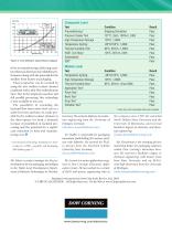
Figure 1. The redistribution layer is achieved by At some point, the holes become too small to print through or too dense to maintain stencil integrity, requiring the use of alternative processes. Cost-sensitive devices with moderateto-low density interconnect patterns, such as memory products, are viewed as ideal candidates for WLP, since the typical chip size and pincounts enable the use of standard, low-cost boards with pitches of 0.65mm and above. The transition to 300mm wafers more than doubles the number of chips per wafer, further reducing cost per die. New Materials printing holds a...
Open the catalog to page 3
less complex than the conventional contact by an array of pins. Low-Contact Resistivity Figure 2. This finite element model shows spiral metallization. the pads from the chip to the bumps is achieved by sputter and plate. The metal stack is applied after structuring a resist with photolithography. The metal stack is situated on top of the bump, making the electrical contact with the interconnect pads in test and assembly. Spiral RDL The plated metal is a Cu/Ni/Au stack, with a high conductivity due to the copper. In addition, because of the gold finish, The metal serves as a reliable...
Open the catalog to page 4
Component Level Test Shipping Simulation Pressure Cooker Test High Temperature Storage Temperature Cycling tivity in manufacturing, delivering excellent thermal, electrical and reliability performance along with the potential for the smallest form factors in packaging. These properties can be reached by using the new resilient contact element combined with a thin-film redistribution layer. Due to the simple process flow and full parallel processing, this technology is now available at low cost. The possibility of extending the backend flow from wafer-level test to a wafer-level test and...
Open the catalog to page 5All Dow Corning catalogs and technical brochures
-
2 part RTV
6 Pages
-
Dow Corning and You Belgium
6 Pages
-
Elastomers from Dow Corning
8 Pages
-
Automotive Airbag
8 Pages
-
Molykote ® 1000
2 Pages
-
Molykote ® L-1210
2 Pages
-
Molykote ® Z Powder
2 Pages
-
Molykote? G-4501
2 Pages
-
Dow Corning Code of Conduct
10 Pages
-
From the Pedal to the Pad
8 Pages
-
MOLYKOTE® 7325
2 Pages
-
MOLYKOTE® MH-62 GREASE
8 Pages
-
MOLYKOTE® 7325 GREASE
2 Pages
-
MOLYKOTE® HP-870
2 Pages
-
MOLYKOTE® 33
4 Pages
-
MOLYKOTE® BG-555
4 Pages
-
MOLYKOTE® G-0050
2 Pages
-
MOLYKOTE® 44
2 Pages
-
Molykote® 1292
2 Pages
-
MOLYKOTE® BR 2
2 Pages
-
Automative
4 Pages
-
Dow Corning Plasma Solutions
2 Pages
-
Design guide to optimize
8 Pages
-
Total Airbag Solutions
8 Pages
-
Adhesives advertisement
2 Pages
Archived catalogs
-
Molykote® Industrial Lubricants
52 Pages


