
- Catalogs
- Diodes Incorporated
- PAM8965

- Products
- Catalogs
- News & Trends
- Exhibitions
PAM8965

PAM8965
The PAM8965 is a high-efficiency Class-D stereo audio amplifier with an integrated synchronous boost converter. It is capable of driving two 12W channels into 4Ω speakers and achieves a system efficiency of 92% at a 7.4V battery voltage. The device features low quiescent and shutdown currents, making it suitable for battery-powered applications.
- Operates from a 2.8V to 8.5V supply.
- Delivers 2x12W into 4Ω load at 7.4V and 2x8W into 6Ω load at 3.7V.
- Includes spread spectrum modulation for EMI suppression and non-clipping power limit with automatic gain control.
- Protection features include under-voltage, over-voltage, short circuit, and thermal shutdown.
- External audio feedback pins for sound customization and Kelvin connection to speaker terminals.
- Lead-free, RoHS compliant, and suitable for automotive applications.
- Portable electronics, Bluetooth and wireless speakers, music instruments, and virtual reality devices.
The document provides detailed pin assignments and descriptions, including fault flag, chip enable, audio inputs, spread spectrum modulation, and power supply connections.
- Input supply voltage ranges from 2.8V to 8.5V.
- System efficiency is 92% at 7.4V with a 4Ω load.
- Quiescent current is 10mA at 7.4V, and shutdown current is 0.7μA.
- Thermal shutdown occurs at 150°C with a 40°C hysteresis.
- Graphs illustrate THD+N vs. power and frequency, frequency response, noise floor, PSRR, crosstalk, efficiency vs. output power, and quiescent current.
- Includes under-voltage and over-voltage protection, short circuit protection, and thermal shutdown.
The PAM8965 operates with a VBAT of 7.4V, a temperature of +25°C, and a load of 4Ω + 33μH. It features a gain set by VDD and supports a VBAT range of 2.8V to 8.5V. The device operates in PWM mode for medium to high loads, transitioning to PFM mode for light loads to improve efficiency. The audio channel has a maximum gain setting of 26dB with low output noise and THD+N. External audio feedback pins allow for customization of sound and elimination of parasitic effects.
The PAM8965 includes a 41-step automatic gain control system, supports single-ended or BTL configurations, and uses spread spectrum modulation to meet EMI specifications. It has a fast start-up time of 15ms and consumes only 0.7μA in the off state. Protection features include under-voltage and over-voltage lockout, short circuit protection, thermal shutdown, and speaker protection.
The device supports differential and single-ended audio inputs, with recommendations for AC-coupling to minimize noise. The audio channel gain is adjustable via the GAIN pin, with a resistor divider setup to define the gain. The EN pin controls enable-disable functions, and the PLIM pin sets a non-clipping power limit to protect speakers. Thermal foldback reduces gain to prevent overheating, and a fault flag indicates abnormal conditions.
The PAM8965 includes under-voltage and over-voltage lockout mechanisms, thermal shutdown, and a fault flag for various fault conditions. The device auto-recovers from UVLO and OVLO conditions.
The PAM8965 device includes an OTP feature that activates when the junction temperature exceeds +150°C, with a hysteresis of +40°C. The system resumes operation once the temperature drops below +110°C. During OTP, both audio channels and the boost converter are turned off, but this is not a latched fault.
The device detects DC signals in the PWM output waveform to prevent speaker damage. If DC is detected, audio channels are turned off and remain off until the fault is cleared by cycling EN or VBAT.
The PAM8965 protects against shorts by disabling audio outputs and entering a Hi-Z state. It auto-recovers after 340ms, but will re-trigger protection if the short persists.
SSM improves EMI performance by randomizing the oscillator frequency. It can be enabled by connecting the SSM pin to a voltage above 1.5V.
To meet FCC Class B regulations, either a ferrite bead filter or a low-pass LC filter can be used. The choice depends on wire length and proximity to sensitive circuits.
The integrated boost converter provides a fixed output voltage of 9.2V and operates in PWM or PFM mode depending on the load. It includes features like cycle-by-cycle current limit and over-voltage protection.
For 1SxP configurations, efficiency is lower, and additional components like a Schottky diode may be needed to manage heat dissipation.
Proper selection of inductors and capacitors is crucial for efficiency and stability. Recommendations include using a 2.2μH inductor with a saturation current rating of at least 10A and specific capacitor values for various pins.
The document provides a typical application circuit for PAM8965 in BTL mode, emphasizing the importance of proper component placement for optimal performance.
The PAM8965 is available in a W-QFN5050-40 package, with specific ordering codes and packaging details provided.
The document specifies the PAM8965 component with a weight of approximately 0.066 grams. The terminals are finished with matte tin-plated leads, solderable per J-STD-002, Test B1. The package type is W-QFN5050-40 (Type US) with detailed dimensions provided in millimeters for various parameters.
Diodes Incorporated provides this document for informational purposes only, without any express or implied warranties. Users are responsible for ensuring the suitability of Diodes products for their applications and compliance with applicable laws and standards. Diodes assumes no liability for application-related information or unauthorized use of the document. The document may contain inaccuracies and is subject to change without notice. The English version is the final and determinative format.
Catalog excerpts

PAM8965 12W STEREO CLASS-D AUDIO AMPLIFIER WITH SYNCHRONOUS BOOST, SSM AND EXTERNAL AUDIO FEEDBACK The PAM8965 is an extremely high-efficiency Class-D stereo audio power amplifier with an integrated synchronous boost converter. The PAM8965 can drive two channels with 12W each into 4Ω speakers. The integrated amplifier can achieve system efficiency of 92% (at VBAT = 7.4V). The device consumes exceptionally low quiescent current (10mA at VBAT = 7.4V) and very low shutdown current (0.7μA). GAIN pin to program audio gain at 0.5dB steps such that external resistors are not required to adjust gain, which can result in gain error. External audio feedback pins, which allow for customization of sound by using feedback network design. Alternatively, these pins can be used for Kelvin connection to speaker terminals. Thermal foldback, which reduces output power as the chip heats up. Non-clipping power limit, which uses 41-step automatic gain control. Spread spectrum modulation (SSM) for EMI suppression (audio and boost), which enables the use of inexpensive ferrite bead filters. The integrated current-mode boost converter provides regulated power to a feature-laden Class-D stereo amplifier. These include: Out-of-audio switching for the boost converter, which minimizes audible noise coming from components on the board. Protection features include under-voltage and over-voltage protection on VBAT, over-voltage protection on PVDD, short circuit protection on all audio outputs, cycle-by-cycle current limit on boost converter, thermal shutdown of the entire system, DC protection for speakers, and an FLT pin that provides a fault flag. Operates from 2.8V to 8.5V Supply 2 12W (10% THD+N) into 4Ω Load with VBAT = 7.4V (2SxP) 2 8W (10% THD+N) into 6Ω Load with VBAT = 3.7V (1SxP) Auto Gain Control Responds to: Thermal Foldback Non-Clip Power Limit GAIN Pin Externally Adjustable Gain from 26dB to 6dB with 0.5dB Steps Exceptionally High Overall System Efficiency (92% @ VBAT = 7.4V) Very Low IQ = 10mA (VBAT = 7.4V) for Boost + Stereo Very Low Shutdown Current = 0.7μA DC Protection for Speaker Auto-Recovery on Short-Circuit Protection & Thermal Shutdown External Audio Feedback Pins Totally Lead-Free & Fully RoHS Compliant (Notes 1 & 2) Halogen and Antimony Free. “Green” Device (Note 3) For automotive applications requiring specific change control (i.e. parts qualified to AEC-Q100/101/200, PPAP capable, and manufactured in IATF 16949 certified facilities), please contact us or your local Diodes representative. https://www.diodes.com/quality/product-definitions/ Portable Electronics Bluetooth Speakers Wireless Speakers Music Instruments High-Capacitance Piezo Actuator Drive Virtual Reality 3D Active Feedback PDA, GPS, Game Machines 1. No purposely added lead. Fully EU Directive 2002/95/EC (RoHS), 2011/65/EU (RoHS 2) & 2015/863/EU (RoHS 3) compliant. 2. See https://www.diodes.com/quality/lead-free/ for more information about Diodes Incorporated’s definitions of Halogen- and Antimony-free, "Green" and Lead-free. 3. Halogen- and Antimony-free "Green” products are defined as those which contain <900ppm bromine, <900ppm chlorine (<1500ppm total Br + Cl) and <1000ppm antimony compounds.
Open the catalog to page 1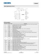
PAM8965 Typical Applications Circuit + RFBP RBSTP ROUTP Right Input Left Input OFF RINN LINP ROUTN RBSTN RFBN LFBP LBSTP LOUTP LOUTN LBSTN LFBN GND Pin Name I/O/P FLT O EN I RINP I RINN I LINN I LINP I SSM I VDD O GND — PLIM I PGND — LFBP I LOUTP O LBSTP P LPVDD P LBSTN P LOUTN O LFBN I PGND SW BST PVDD VBAT2 VBAT1 PGND RFBN ROUTN RBSTN RPVDD RBSTP ROUTP RFBP GND Description Fault flag. Open-drain output to signal system faults (VBAT UVLO or OVLO, OTP, DC input, audio SCP) Chip enable. High = ON, Low = OFF. Do not float this pin. Right channel audio input – Positive Right channel audio input...
Open the catalog to page 2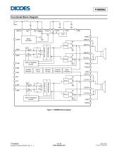
PAM8965 Functional Block Diagram VBAT Boost Converter Sample & Hold Driver PLIM RFBN PGND UVLO / OVLO ON/OFF De-pop Thermal Protection Short Protection LFBP LBSTP Sample & Hold Driver AGC & Feedback Control LFBN PGND Figure 1. PAM8965 Block Diagram
Open the catalog to page 3
PAM8965 Absolute Maximum Ratings (@TA = +25° unless otherwise specified.) (Note 4) C, Symbol Audio Input Voltage VRINP, VRINN, VLINP, VLINN Supply Voltage (Pins VBAT1, VBAT2) VPLIM, VGAIN, VSSM Control Input Voltage Control Input Voltage Maximum Operating Junction Temperature (Note 5) Storage Temperature Range Human Body Model Charged Device Model Stresses greater than the Absolute Maximum Ratings specified above can cause permanent damage to the device. These are stress ratings only; functional operation of the device at these or any other conditions exceeding those indicated in this specification...
Open the catalog to page 4
PAM8965 Electrical Characteristics (VBAT = 7.4V, TA = +25° RL = 4Ω + 2 33μH, VPLIM = VGAIN = VDD, unless otherwise specified.) C, Symbol Test Condition Input Supply Voltage High-Level Input Voltage Low-Level Input Voltage VBAT Rising VBAT Falling System Efficiency (Boost + Stereo) Quiescent Current Shutdown Current VBAT Falling VBAT Rising VBAT OVLO Threshold VBAT UVLO Threshold Thermal Shutdown Threshold Thermal Shutdown Hysteresis Thermal Foldback Trip Point Boost Converter (VBAT = 7.4V, TA = +25° RL = 4Ω + 2 33μH, VPLIM = VGAIN = VDD, unless otherwise specified.) C, Symbol Test Condition...
Open the catalog to page 5
PAM8965 Class-D Amplifier (VBAT = 7.4V, TA = +25° RL = 4Ω + 2 33μH, VPLIM = VGAIN = VDD, unless otherwise specified.) C, Symbol Continuous Output Power, 1SxP (per Channel) (Note 7) THD+N Total Harmonic Distortion + Noise Integrated Output Noise Power Supply Rejection Ratio Signal-to-Noise Ratio Gain = 20dB VIN @ AC Ground, 20Hz to 22kHz SSM Off Gain = 26dB VIN @ AC Ground, 20Hz to 22kHz SSM Off VIN = AC Ground ±100mV Supply Ripple Gain = 26dB THD+N = 1%, Gain = 26dB, A-Weighted, SSM Off Continuous Output Power, 2SxP (per Channel) (Note 6) Test Condition Output Offset Voltage Audio Oscillator...
Open the catalog to page 6All Diodes Incorporated catalogs and technical brochures
 ZXCT21x
2 Pages
 ZXCT21x
15 Pages
 PI2MEQX2503
16 Pages
 AP43781
2 Pages
 APR3401
9 Pages
 AP3306
13 Pages
 AP3306
2 Pages
 AP43771H
9 Pages
 PAM8907
10 Pages
 AP22953
12 Pages
 PI6LC58S1101
17 Pages
 PI3EQX12902E
1 Page
 AP22653Q
13 Pages
 Protection Products
2 Pages
 LOGIC PRODUCTS
20 Pages
 MOSFETS
20 Pages
 automotive products
20 Pages
 PRODUCT OVERVIEW
2 Pages
 Logic single gate 74AHC1G00
8 Pages
 AMR sensor angular ZMT32
10 Pages
 Audio amplifiers PAM8001
17 Pages
 Off-line LED drivers AL9910
15 Pages
 Operational amplifiers AP358
16 Pages
 Buck converter AP1501
12 Pages
 MOSFETs N Channel DMG1012T
6 Pages
 Bipolar transistor 2DA2018
5 Pages
 Schottky diodes 1N5711WS
3 Pages
 SENSORS AND MOTOR CONTROL
12 Pages
 LED Driver
16 Pages
 STANDARD LINEAR AND LOGIC
12 Pages
 Power Management
12 Pages
 BIPOLAR TRANSISTORS
24 Pages
 SBR®
SBR®12 Pages
 MOSFETs
16 Pages


Archived catalogs
 Diodes Product Design Guide
173 Pages

- Temperature probe
- Resistance temperature sensor
- Signal amplifying integrated circuit
- Motor controller
- Transceiver module
- Rotary electric switch
- RTD temperature sensor
- DC motor controller
- Transistor module
- Signal conditioner
- Rectifier diode
- DC amplifier
- On/off switch
- Radio transceiver module
- Brushless motor control
- Avalanche diode
- Switching transistor
- Electronic amplifier