- Catalogs
- Diodes Incorporated
- Operational amplifiers AP358
Operational amplifiers AP358
1 /16Pages

Operational amplifiers AP358
1 /16Pages
Catalog excerpts
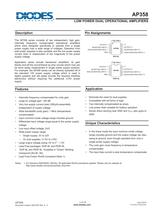
AP358 LOW POWER DUAL OPERATIONAL AMPLIFIERS The AP358 series consists of two independent, high gain, internally frequency compensated operational amplifiers which were designed specifically to operate from a single power supply over a wide range of voltages. Operation from split power supplies is also possible and the low power supply current drain is independent of the magnitude of the power supply voltage. ( Top View ) OUTPUT 1 INVERTING INPUT 1 NON-INVERTING INPUT 1 OUTPUT 2 INVERTING INPUT 2 Application areas include transducer amplifiers, dc gain blocks and all the conventional op amp circuits which now can be more easily implemented in single power supply systems. For example, the AP358 series can be directly operated off of the standard +5V power supply voltage which is used in digital systems and will easily provide the required interface electronics without requiring the additional ±15V power supply. ( Top View ) OUTPUT 1 INVERTING INPUT 1 NON-INVERTING INPUT 1 Internally frequency compensated for unity gain Large dc voltage gain: 100 dB Very low supply current drain (500μA)-essentially independent of supply voltage Wide bandwidth (unity gain): 1 MHz (temperature compensated) Input common-mode voltage range includes ground Differential input voltage range equal to the power supply voltage Low input offset voltage: 2mV Wide power supply range: • Unique Characteristics • • Or dual supplies: ±1.5V to ±16V + Large output voltage swing: 0V to V - 1.5V Lead Free packages: SOP-8L and PDIP-8L SOP-8L and PDIP-8L: Available in “Green” Molding Compound (No Br, Sb) Lead Free Finish/ RoHS Compliant (Note 1) Eliminate the need for dual supplies Compatible with all forms of logic Two internally compensated op amps Low power drain suitable for battery operation Allows direct sensing near GND and VOUT also goes to GND In the linear mode the input common-mode voltage range includes ground and the output voltage can also swing to ground, even though operated from only a single power supply voltage. The unity gain cross frequency is temperature compensated. The input bias current is also temperature compensate. 1. EU Directive 2002/95/EC (RoHS). All applicable RoHS exemptions applied. Please visit our website at http://www.diodes.com/products/lead_free.html. July 2010 © Diodes Incorporated
Open the catalog to page 1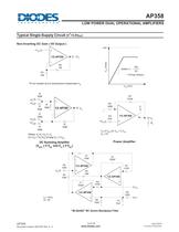
AP358 LOW POWER DUAL OPERATIONAL AMPLIFIERS Typical Single-Supply Circuit (V+=5.0VDC) Non-Inverting DC Gain ( 0V Output ) * *R not needed due to temperature independent IIN Power Amplifier DC Summing Amplifier (VIN'S > 0 VDC and VO > 0 VDC) R1 100K "BI-QUAD" RC Active Bandpass Filter July 2010 © Diodes Incorporated
Open the catalog to page 2
AP358 LOW POWER DUAL OPERATIONAL AMPLIFIERS Typical Single-Supply Circuit (Continued) (V+=5.0VDC) V+ Current Monitor Fixed Current Sources Lamp Driver Voltage Follower Squarewave Oscillator Pulse Generator July 2010 © Diodes Incorporated
Open the catalog to page 3
AP358 LOW POWER DUAL OPERATIONAL AMPLIFIERS Typical Single-Supply Circuit (Continued) (V+=5.0VDC) IB AUX AMP INPUT CURRENT COMPENSATION Low Drift Peak Detector R1 30K IO =0.1 amp / volt VIN (increase RE for IO small) High Compliance Current Sink *WIDE CONTROL VOLTAGE RANGE: 0 VDC < VC < 2 (V+ -1.5VDC) Voltage Controlled Oscillator (VCO) July 2010 © Diodes Incorporated
Open the catalog to page 4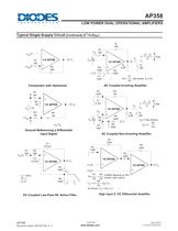
AP358 LOW POWER DUAL OPERATIONAL AMPLIFIERS Typical Single-Supply Circuit (Continued) (V+=5.0VDC) Rf 10K R1 CIN 10K +V2 R4 (CMRR depends on this R3 resistor ratio match) R4 V O = (1+ )(V2-V1) R3 As Shown: VO = 2(V2-V1) For DC Coupled Low-Pass RC Active Filter AC Coupled Non-Inverting Amplifier Ground Referencing a Differential Input Signal AC Coupled Inverting Amplifier Comparator with Hysteresis High Input Z, DC Differential Amplifier July 2010 © Diodes Incorporated
Open the catalog to page 5
AP358 LOW POWER DUAL OPERATIONAL AMPLIFIERS Typical Single-Supply Circuit (Continued) (V+=5.0VDC) C1 0.01μF R1 390K V IN Bandpass Active Filter R2 100K GAIN ADJUST If R1 = R5 & R3 = R4 = R6 = R7 (CMRR depends on match) 2R2 )(V2-V1) V O =( 1+ R1 As Shown: VO = 101(V2-V1) High Input Z Adjustable-Gain DC Instrumentation Amplifier AUX AMP INPUT CURRENT COMPENSATION Using Symmetrical Amplifiers to Reduce Input Current (General Concept) July 2010 © Diodes Incorporated
Open the catalog to page 6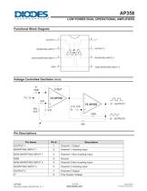
AP358 LOW POWER DUAL OPERATIONAL AMPLIFIERS Functional Block Diagram Voltage Controlled Oscillator (VCO) R 100K Pin Descriptions Pin Name OUTPUT 1 Channel 1 Inverting Input Channel 1 Non-inverting Input Ground Channel 2 Non-inverting Input Channel 2 Inverting Input Channel 2 Output Chip Supply Voltage Description Channel 1 Output July 2010 © Diodes Incorporated
Open the catalog to page 7
AP358 LOW POWER DUAL OPERATIONAL AMPLIFIERS Absolute Maximum Ratings Symbol VCC VIN PD Parameter Supply voltage Differential Input Voltage Input Voltage Power Dissipation (Note 2) Output Short-Circuit to GND (One Amplifier) (Note 3) V+ < 15V and TA=25oC Input Current (VIN < -0.3V) (Note 4) Operating Temperature Range Storage Temperature Range 2. For operating at high temperatures, the AP358 must be derated based on a +125°C maximum junction temperature and a thermal resistance of 120°C/W for DIP and 189°C/W for Small Outline package, which applies for the device soldered in a printed circuit...
Open the catalog to page 8
AP358 LOW POWER DUAL OPERATIONAL AMPLIFIERS Electrical Characteristics (TA = 25oC, V+ = +5.0V, unless otherwise stated) (Note 5) Symbol VIO IB IIO VICM IS AV CMRR PSRR Parameter Input Offset Voltage Conditions TA = 25oC, (Note 6) IIN(+) or IIN(−), TA = 25°C, Input Bias Current VCM = 0V, (Note 7) IIN(+) - IIN(−),VCM = 0V, Input Offset Current TA = 25°C V+ = 30V, (Note 8) Input Common-Mode Voltage Range TA = 25°C RL = ∞ on V+ = 30V Supply Current All Op Over Full Temperature Range V+ = 5V Amps V+ = 15V, TA = 25°C, Large Signal Voltage Gain RL > 2kΩ, (For VO = 1V to 11V) TA = 25°C, VCM = 0V to Common-Mode...
Open the catalog to page 9
AP358 LOW POWER DUAL OPERATIONAL AMPLIFIERS Electrical Characteristics (Continued) Symbol Conditions VIN = 1V, VIN+ = 0V, V+ = 15V, VO = 2V, TA = 25°C VIN- = 1V, VIN+ = 0V, V+ = 15V, VO = 200mV, TA = 25°C VIN+ = 1V, VIN- = 0V, V+ = 15V, VO = 2V, TA = 25°C TA = 25°C, (Note 3) V+ = 15V RL = 2kΩ, TA = 25oC RL = 10kΩ, TA = 25oC RL = 10kΩ, TA = 25oC Sink Output Current Source Short Circuit to Ground Output Voltage Swing 3. Short circuits from the output to V can cause excessive heating and eventual destruction. When considering short circuits + to ground, the maximum output current is approximately...
Open the catalog to page 10All Diodes Incorporated catalogs and technical brochures
 ZXCT21x
2 Pages
 ZXCT21x
15 Pages
 PI2MEQX2503
16 Pages
 AP43781
2 Pages
 APR3401
9 Pages
 AP3306
13 Pages
 AP3306
2 Pages
 AP43771H
9 Pages
 PAM8907
10 Pages
 AP22953
12 Pages
 PI6LC58S1101
17 Pages
 PI3EQX12902E
1 Page
 AP22653Q
13 Pages
 PAM8965
25 Pages
 Protection Products
2 Pages
 LOGIC PRODUCTS
20 Pages
 MOSFETS
20 Pages
 automotive products
20 Pages
 PRODUCT OVERVIEW
2 Pages
 Logic single gate 74AHC1G00
8 Pages
 AMR sensor angular ZMT32
10 Pages
 Audio amplifiers PAM8001
17 Pages
 Off-line LED drivers AL9910
15 Pages
 Buck converter AP1501
12 Pages
 MOSFETs N Channel DMG1012T
6 Pages
 Bipolar transistor 2DA2018
5 Pages
 Schottky diodes 1N5711WS
3 Pages
 SENSORS AND MOTOR CONTROL
12 Pages
 LED Driver
16 Pages
 STANDARD LINEAR AND LOGIC
12 Pages
 Power Management
12 Pages
 BIPOLAR TRANSISTORS
24 Pages
 SBR®
SBR®12 Pages
 MOSFETs
16 Pages


Archived catalogs
 Diodes Product Design Guide
173 Pages

- Temperature probe
- Resistance temperature sensor
- Proximity switch
- Technology switch
- Signal amplifying integrated circuit
- Transceiver module
- Motor controller
- Rotary electric switch
- RTD temperature sensor
- DC motor controller
- Transistor module
- Touch switch
- Signal conditioner
- Magnetic proximity sensor
- Rectifier diode
- DC amplifier
- On/off switch
- Radio transceiver module