- Catalogs
- Diodes Incorporated
- Logic single gate 74AHC1G00
Logic single gate 74AHC1G00
1 /8Pages

Logic single gate 74AHC1G00
1 /8Pages
Catalog excerpts
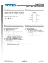
74AHC1G00 SINGLE 2 INPUT POSITIVE NAND GATE The 74AHC1G00 is a single 2-input positive NAND gate with a standard push-pull output. The device is designed for operation with a power supply range of 2.0 V to 5.5 V. The gate performs the positive Boolean function: Supply Voltage Range from 2.0V to 5.5V General Purpose Logic Wide array of products such as: CMOS low power consumption PCs, networking, notebooks, netbooks, PDAs Schmitt Trigger Action at All Inputs Make the Circuit Computer peripherals, hard drives, CD/DVD ROM Tolerant for Slower Input Rise and Fall Time. MP3 players ,Cameras, Video Recorders Exceeds 2000-V Human Body Model (A114-A) Exceeds 200-V Machine Model (A115-A) Exceeds 1000-V Charged Device Model (C101C) Latch-Up Exceeds 100mA per JESD 78, Class II SOT25 and SOT353: Assembled with “Green” Molding Compound (no Br, Sb) Lead Free Finish / RoHS Compliant (Note 1) 1. EU Directive 2002/95/EC (RoHS). All applicable RoHS exemptions applied. Please visit our website at http://www.diodes.com/products/lead_free.html. March 2011 © Diodes Incorporated
Open the catalog to page 1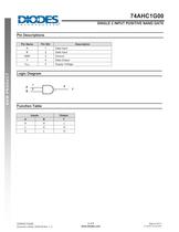
74AHC1G00 SINGLE 2 INPUT POSITIVE NAND GATE Pin Descriptions Pin NO. Data Input Data Input Ground Data Output Supply Voltage Logic Diagram Function Table March 2011 © Diodes Incorporated
Open the catalog to page 2
74AHC1G00 SINGLE 2 INPUT POSITIVE NAND GATE Absolute Maximum Ratings (Note 2) Symbol ESD HBM ESD CDM ESD MM VCC Human Body Model ESD Protection Charged Device Model ESD Protection Machine Model ESD Protection Input Voltage Range Supply Voltage Range Voltage applied to output in high or low state Input Clamp Current VI<0 Output Clamp Current (VO < 0 or VO > VCC) Continuous output current (VO = 0 to VCC) Continuous current through VCC Continuous current through GND Operating Junction Temperature Storage Temperature TSTG Notes: 2. Stresses beyond the absolute maximum may result in immediate failure...
Open the catalog to page 3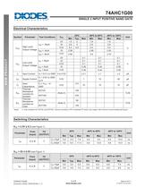
74AHC1G00 SINGLE 2 INPUT POSITIVE NAND GATE Electrical Characteristics Symbol Test Conditions High Level Output Voltage I = -4mA OH Low Level Output Voltage Input Current Supply Current Input Capacitance Thermal Resistance Junction-toAmbient Thermal Resistance Junction-toCase 4. Test conditions for SOT25, and SOT353: Device mounted on FR-4 substrate PC board, 2oz copper, with minimum recommended pad layout Switching Characteristics VCC = 3.3V ± 0.3 (see Figure 1) Parameter March 2011 © Diodes Incorporated
Open the catalog to page 4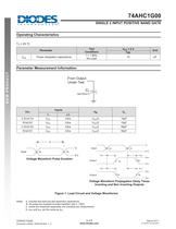
74AHC1G00 SINGLE 2 INPUT POSITIVE NAND GATE Operating Characteristics TA = 25 ºC Parameter Power dissipation capacitance Test Conditions f = 1 MHz No Load Parameter Measurement Information Voltage Waveform Pulse Duration Voltage Waveform Propagation Delay Times Inverting and Non Inverting Outputs Figure 1. Load Circuit and Voltage Waveforms Notes: A. Includes test lead and test apparatus capacitance. B. All pulses are supplied at pulse repetition rate ≤ 1 MHz. C. Inputs are measured separately one transition per measurement. D. tPLH and tPHL are the same as tPD. March 2011 © Diodes Incorporated...
Open the catalog to page 5
74AHC1G00 SINGLE 2 INPUT POSITIVE NAND GATE Ordering Information Logic Device 74 : Logic Prefix AHC : 2 to 5.5V Family 1G : One gate Device 74AHC1G00W5-7 74AHC1G00SE-7 Notes: Packing 7 : Tape & Reel 7” Tape and Reel Quantity Part Number Suffix 3000/Tape & Reel -7 3000/Tape & Reel -7 5. Pad layout as shown on Diodes Inc. suggested pad layout document AP02001, which can be found on our website at http://www.diodes.com/datasheets/ap02001.pdf. Marking Information (Top View) XX : Identification code Y : Year 0~9 W : Week : A~Z : 1~26 week; a~z : 27~52 week; z represents 52 and 53 week X : A~Z : Internal...
Open the catalog to page 6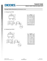
74AHC1G00 SINGLE 2 INPUT POSITIVE NAND GATE Package Outline Dimensions (All Dimensions in mm) (1) Package Type: SOT25 A March 2011 © Diodes Incorporated
Open the catalog to page 7
74AHC1G00 SINGLE 2 INPUT POSITIVE NAND GATE IMPORTANT NOTICE DIODES INCORPORATED MAKES NO WARRANTY OF ANY KIND, EXPRESS OR IMPLIED, WITH REGARDS TO THIS DOCUMENT, INCLUDING, BUT NOT LIMITED TO, THE IMPLIED WARRANTIES OF MERCHANTABILITY AND FITNESS FOR A PARTICULAR PURPOSE (AND THEIR EQUIVALENTS UNDER THE LAWS OF ANY JURISDICTION). Diodes Incorporated and its subsidiaries reserve the right to make modifications, enhancements, improvements, corrections or other changes without further notice to this document and any product described herein. Diodes Incorporated does not assume any liability arising...
Open the catalog to page 8All Diodes Incorporated catalogs and technical brochures
 ZXCT21x
2 Pages
 ZXCT21x
15 Pages
 PI2MEQX2503
16 Pages
 AP43781
2 Pages
 APR3401
9 Pages
 AP3306
13 Pages
 AP3306
2 Pages
 AP43771H
9 Pages
 PAM8907
10 Pages
 AP22953
12 Pages
 PI6LC58S1101
17 Pages
 PI3EQX12902E
1 Page
 AP22653Q
13 Pages
 PAM8965
25 Pages
 Protection Products
2 Pages
 LOGIC PRODUCTS
20 Pages
 MOSFETS
20 Pages
 automotive products
20 Pages
 PRODUCT OVERVIEW
2 Pages
 AMR sensor angular ZMT32
10 Pages
 Audio amplifiers PAM8001
17 Pages
 Off-line LED drivers AL9910
15 Pages
 Operational amplifiers AP358
16 Pages
 Buck converter AP1501
12 Pages
 MOSFETs N Channel DMG1012T
6 Pages
 Bipolar transistor 2DA2018
5 Pages
 Schottky diodes 1N5711WS
3 Pages
 SENSORS AND MOTOR CONTROL
12 Pages
 LED Driver
16 Pages
 STANDARD LINEAR AND LOGIC
12 Pages
 Power Management
12 Pages
 BIPOLAR TRANSISTORS
24 Pages
 SBR®
SBR®12 Pages
 MOSFETs
16 Pages


Archived catalogs
 Diodes Product Design Guide
173 Pages

- Bourn And Koch temperature sensor
- Bourn And Koch resistance temperature sensor
- Bourn And Koch proximity sensor
- Technology switch
- Bourn And Koch signal amplifier
- Bourn And Koch transceiver
- Motor controller
- Rotary electric switch
- RTD temperature sensor
- Bourn And Koch power amplifier
- DC motor controller
- Bourn And Koch transistor
- Touch switch
- Signal conditioner
- Bourn And Koch magnetic proximity sensor
- Rectifier diode
- DC amplifier
- On/off switch
- Bourn And Koch radio transceiver