- Catalogs
- Diodes Incorporated
- Bipolar transistor 2DA2018
Bipolar transistor 2DA2018
1 /5Pages

Bipolar transistor 2DA2018
1 /5Pages
Catalog excerpts
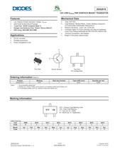
2DA2018 12V LOW VCE(sat) PNP SURFACE MOUNT TRANSISTOR ADVANCE INFORMATION Mechanical Data Low Collector-Emitter Saturation Voltage, VCE(sat) Ultra-Small Surface Mount Package “Lead Free”, RoHS Compliant (Note 1) Halogen and Antimony Free. "Green" Device (Note 2) ESD rating: 400V-MM, 8KV-HBM Case: SOT-523 Case Material: Molded Plastic, “Green” Molding Compound. UL Flammability Classification Rating 94V-0 Moisture Sensitivity: Level 1 per J-STD-020 Terminals: Matte Tin Finish annealed over Alloy 42 leadframe (Lead Free Plating) Solderable per MIL-STD-202, Method 208 Terminal Connections: See Diagram Weight: 0.002 grams (approximate) DC-DC converter Portable equipments Power management units Device Symbol Ordering Information (Note 3) Product 2DA2018-7 Notes: Reel size (inches) 7 1. No purposefully added lead. 2. Diodes Inc’s “Green” Policy can be found on our website at http://www.diodes.com 3. For packaging details, go to our website at http://www.diodes.com Marking Information Date Code Key Year Code Month Code KTF = Product Type Marking Code YM = Date Code Marking Y = Year (ex: W = 2009) M = Month (ex: 9 = September) October 2010 © Diodes Incorporated
Open the catalog to page 1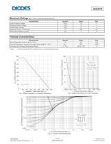
Characteristic Collector-Base Voltage Collector-Emitter Voltage Emitter-Base Voltage Collector Current - Continuous Peak Pulse Collector Current Symbol VCBO VCEO VEBO IC ICM Symbol PD RθJA TJ, TSTG Thermal Characteristics Characteristic Power Dissipation (Note 4) @ TA = 25°C Thermal Resistance, Junction to Ambient (Note 4) @ TA = 25°C Operating and Storage Temperature Range Notes: 4. Device mounted on FR-4 PCB with minimum recommended pad layout. 160 P(pk), PEAK TRANSIENT POWER (W) Single Pulse RθJA(t) = r(t) * RθJA RθJA = 470°C/W TJ - TA = P * RθJA(t) Duty Cycle, D = t1/t2 20 40 60 80 100 120...
Open the catalog to page 2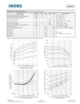
2DA2018 Electrical Characteristics @TA = 25°C unless otherwise specified Symbol BVCBO BVCEO BVEBO Collector Cutoff Current Emitter Cutoff Current DC Current Gain (Note 5) Collector-Emitter Saturation Voltage (Note 5) Output Capacitance Current Gain-Bandwidth Product Turn-On Time Delay Time Rise Time Turn-Off Time Storage Time Fall Time VCE(sat) Cobo fT ton td tr toff ts tf 5. Measured under pulsed conditions. Pulse width = 300μs. Duty cycle ≤2%. 1 10 100 1,000 IC, COLLECTOR CURRENT (mA) Fig. 5 Typical DC Current Gain vs. Collector Current 2 4 6 8 10 VCE, COLLECTOR-EMITTER VOLTAGE (V) Fig. 4 Typical...
Open the catalog to page 3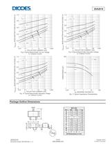
VBE(SAT), BASE-EMITTER SATURATION VOLTAGE (V) VBE(ON), BASE-EMITTER TURN-ON VOLTAGE (V) 0.1 1 10 100 1,000 IC, COLLECTOR CURRENT (mA) Fig. 8 Typical Base-Emitter Turn-On Voltage vs. Collector Current 0.1 1 10 100 1,000 IC, COLLECTOR CURRENT (mA) Fig. 9 Typical Base-Emitter Saturation Voltage vs. Collector Current VBE(SAT), BASE-EMITTER SATURATION VOLTAGE (V) ADVANCE INFORMATION 0.1 1 10 100 1,000 IC, COLLECTOR CURRENT (mA) Fig. 10 Typical Base-Emitter Saturation Voltage vs. Collector Current 0.1 1 10 100 VR, REVERSE VOLTAGE (V) Fig. 11 Typical Capacitance Characteristics Package Outline Dimensions...
Open the catalog to page 4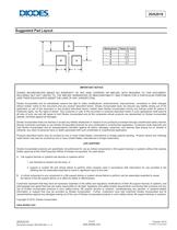
ADVANCE INFORMATION IMPORTANT NOTICE DIODES INCORPORATED MAKES NO WARRANTY OF ANY KIND, EXPRESS OR IMPLIED, WITH REGARDS TO THIS DOCUMENT, INCLUDING, BUT NOT LIMITED TO, THE IMPLIED WARRANTIES OF MERCHANTABILITY AND FITNESS FOR A PARTICULAR PURPOSE (AND THEIR EQUIVALENTS UNDER THE LAWS OF ANY JURISDICTION). Diodes Incorporated and its subsidiaries reserve the right to make modifications, enhancements, improvements, corrections or other changes without further notice to this document and any product described herein. Diodes Incorporated does not assume any liability arising out of the application...
Open the catalog to page 5All Diodes Incorporated catalogs and technical brochures
 ZXCT21x
2 Pages
 ZXCT21x
15 Pages
 PI2MEQX2503
16 Pages
 AP43781
2 Pages
 APR3401
9 Pages
 AP3306
13 Pages
 AP3306
2 Pages
 AP43771H
9 Pages
 PAM8907
10 Pages
 AP22953
12 Pages
 PI6LC58S1101
17 Pages
 PI3EQX12902E
1 Page
 AP22653Q
13 Pages
 PAM8965
25 Pages
 Protection Products
2 Pages
 LOGIC PRODUCTS
20 Pages
 MOSFETS
20 Pages
 automotive products
20 Pages
 PRODUCT OVERVIEW
2 Pages
 Logic single gate 74AHC1G00
8 Pages
 AMR sensor angular ZMT32
10 Pages
 Audio amplifiers PAM8001
17 Pages
 Off-line LED drivers AL9910
15 Pages
 Operational amplifiers AP358
16 Pages
 Buck converter AP1501
12 Pages
 MOSFETs N Channel DMG1012T
6 Pages
 Schottky diodes 1N5711WS
3 Pages
 SENSORS AND MOTOR CONTROL
12 Pages
 LED Driver
16 Pages
 STANDARD LINEAR AND LOGIC
12 Pages
 Power Management
12 Pages
 BIPOLAR TRANSISTORS
24 Pages
 SBR®
SBR®12 Pages
 MOSFETs
16 Pages


Archived catalogs
 Diodes Product Design Guide
173 Pages

- Temperature probe
- Resistance temperature sensor
- Proximity switch
- Technology switch
- Signal amplifying integrated circuit
- Transceiver module
- Motor controller
- Rotary electric switch
- RTD temperature sensor
- Power amplifying integrated circuit
- DC motor controller
- Touch switch
- Signal conditioner
- Magnetic proximity sensor
- Rectifier diode
- DC amplifier
- On/off switch
- Radio transceiver module