- Catalogs
- Diodes Incorporated
- APR3401
APR3401
1 /9Pages

APR3401
1 /9Pages
Catalog excerpts

Lead-free Green APR3401 SECONDARY SIDE SYNCHRONOUS RECTIFICATION CONTROLLER Description Pin Assignments The APR3401 is a secondary side MOSFET driver for synchronous rectification in DCM/QR/ACF operation. The synchronous rectification can effectively reduce the secondary side rectifier power dissipation and provide high-performance solution. By sensing primary MOSFET gate-to-source voltage, the APR3401 can output ideal drive signal with less external components. The APR3401 is available in the SOT26 package. Features AREF GND VDET • Adapters/chargers for cells/cordless phones, ADSL modems, MP3 and other portable apparatus Synchronous Rectification for DCM/QR/ACF Operation Flyback Eliminate Resonant Ring Interference Fewest External Components Totally Lead-Free & Fully RoHS Compliant (Notes 1 & 2) Halogen and Antimony Free. “Green” Device (Note 3) For automotive applications requiring specific change control (i.e. parts qualified to AEC-Q100/101/104/200, PPAP capable, and manufactured in IATF 16949 certified facilities), please contact us or your local Diodes representative. https://www.diodes.com/quality/product-definitions/ Notes: 1. No purposely added lead. Fully EU Directive 2002/95/EC (RoHS), 2011/65/EU (RoHS 2) & 2015/863/EU (RoHS 3) compliant. 2. See https://www.diodes.com/quality/lead-free/ for more information about Diodes Incorporated’s definitions of Halogen- and Antimony-free, "Green" and Lead-free. 3. Halogen- and Antimony-free "Green” products are defined as those which contain <900ppm bromine, <900ppm chlorine (<1500ppm total Br + Cl) and <1000ppm antimony compounds. August 2023 2023 Copyright Diodes Incorporated. All Rights Reserved.
Open the catalog to page 1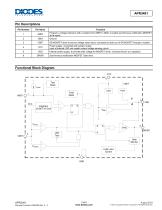
Pin DescriptionsFunctional Block Diagram APR3401 August 2023 2023 Copyright Diodes Incorporated. All Rights Reserved.
Open the catalog to page 2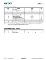
Absolute Maximum Ratings (Note 4) Symbol Notes: 4. Stresses greater than those listed under Absolute Maximum Ratings can cause permanent damage to the device. These are stress ratings only, and functional operation of the device at these or any other conditions beyond those indicated under Recommended Operating Conditions is not implied. Exposure to Absolute Maximum Ratings for extended periods can affect device reliability. 5. The aging condition of VDET pin is 80% of AMR value. Recommended Operating Conditions Symbol August 2023 2023 Copyright Diodes Incorporated. All Rights Reserved.
Open the catalog to page 3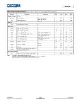
Electrical Characteristics (@ Vcc = 5V, Ta = -40°C < Ta < +85°C, unless otherwise specified.) Notes: 6. This item is used to specify the value of Raref. 7. This item specifies the minimum SR operating voltage of Vin_dc, Vin_dc ^ Nps*Vs_min. 8. These parameters are guaranteed by design and characterization. August 2023 2023 Copyright Diodes Incorporated. All Rights Reser
Open the catalog to page 4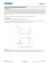
APR3401 Synchronous Rectification Principle Description SR MOSFET Turn On The APR3401 determines the synchronous rectification MOSFET turn-on time by monitoring the MOSFET drain-to-source voltage. When the drain voltage is lower than the turn-on threshold voltage VTHON, the IC outputs a positive drive voltage after a turn-on delay time (tDON). The MOSFET will turn on and the current will transfer from the body diode into the MOSFET’s channel. Because of the parasitic parameter, the voltage on the MOSFET drain pin may have a moderate voltage ringing at this moment, which may impact the VDET voltage...
Open the catalog to page 5
APR3401 Synchronous Rectification Principle Description (continued) The Value and Meaning of AREF Resistor As to the DCM operation flyback converter—after the secondary rectifier stops conducting, the resonance of the primary inductance and output capacitance of the equivalent switch device creates the primary MOSFET drain-to-source ringing waveform. This ringing waveform may lead to Synchronous Rectifier error conduction. To avoid this fault occurrence, the APR3401 has a special function by means of volt-second product detecting. Regarding the sensed voltage of the VDET pin, the volt-second...
Open the catalog to page 6
Synchronous Rectification Principle Description Vdd The Vdd is the output voltage of the Pulse Linear Regulator (PLR) or the Low Dropout Regulator (LDO). It provides bias voltage for the controller. A capacitor (typically 4.7pF) should be connected between the VDD pin and GND pin. XX : Identification Code Y : Year 0 to 9 (ex: 3 = 2023) W : Week : A to Z : Week 1 to 26; a to z : Week 27 to 52; z Represents Week 52 and 53 X : Internal Code August 2023 2023 Copyright Diodes Incorporated. All Rights Reserved.
Open the catalog to page 7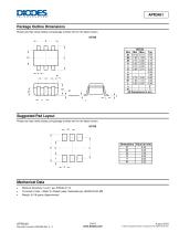
Package Outline Dimensions Please see http://www.diodes.com/package-outlines.html for the latest version. SOT26 Suggested Pad Layout_ Please see http://www.diodes.com/package-outlines.html for the latest version. SOT26 Mechanical Data • Moisture Sensitivity: Level 1 per JESD22-A113 • Terminals: Finish - Matte Tin Plated Leads, Solderable per JESD22-B102 (H) • Weight: 0.018 grams (Approximate) APR3401 August 2023 2023 Copyright Diodes Incorporated. All Rights Reserved.
Open the catalog to page 8
IMPORTANT NOTICE 1. DIODES INCORPORATED (Diodes) AND ITS SUBSIDIARIES MAKE NO WARRANTY OF ANY KIND, EXPRESS OR IMPLIED, WITH REGARDS TO ANY INFORMATION CONTAINED IN THIS DOCUMENT, INCLUDING, BUT NOT LIMITED TO, THE IMPLIED WARRANTIES OF MERCHANTABILITY, FITNESS FOR A PARTICULAR PURPOSE OR NON-INFRINGEMENT OF THIRD PARTY INTELLECTUAL PROPERTY RIGHTS (AND THEIR EQUIVALENTS UNDER THE LAWS OF ANY JURISDICTION). 2. The Information contained herein is for informational purpose only and is provided only to illustrate the operation of Diodes’ products described herein and application examples. Diodes...
Open the catalog to page 9All Diodes Incorporated catalogs and technical brochures
 ZXCT21x
2 Pages
 ZXCT21x
15 Pages
 PI2MEQX2503
16 Pages
 AP43781
2 Pages
 AP3306
13 Pages
 AP3306
2 Pages
 AP43771H
9 Pages
 PAM8907
10 Pages
 AP22953
12 Pages
 PI6LC58S1101
17 Pages
 PI3EQX12902E
1 Page
 AP22653Q
13 Pages
 PAM8965
25 Pages
 Protection Products
2 Pages
 LOGIC PRODUCTS
20 Pages
 MOSFETS
20 Pages
 automotive products
20 Pages
 PRODUCT OVERVIEW
2 Pages
 Logic single gate 74AHC1G00
8 Pages
 AMR sensor angular ZMT32
10 Pages
 Audio amplifiers PAM8001
17 Pages
 Off-line LED drivers AL9910
15 Pages
 Operational amplifiers AP358
16 Pages
 Buck converter AP1501
12 Pages
 MOSFETs N Channel DMG1012T
6 Pages
 Bipolar transistor 2DA2018
5 Pages
 Schottky diodes 1N5711WS
3 Pages
 SENSORS AND MOTOR CONTROL
12 Pages
 LED Driver
16 Pages
 STANDARD LINEAR AND LOGIC
12 Pages
 Power Management
12 Pages
 BIPOLAR TRANSISTORS
24 Pages
 SBR®
SBR®12 Pages
 MOSFETs
16 Pages


Archived catalogs
 Diodes Product Design Guide
173 Pages

- Temperature probe
- Resistance temperature sensor
- Proximity switch
- Technology switch
- Signal amplifying integrated circuit
- Transceiver module
- Motor controller
- Rotary electric switch
- RTD temperature sensor
- Power amplifying integrated circuit
- DC motor controller
- Transistor module
- Touch switch
- Signal conditioner
- Magnetic proximity sensor
- Rectifier diode
- DC amplifier
- On/off switch
- Radio transceiver module