- Catalogs
- Diodes Incorporated
- AP22953
AP22953
1 /12Pages

AP22953
1 /12Pages
Catalog excerpts

AP22953 SWITCH FOR VBUS LINE WITH OVERVOLTAGE, SURGE, AND ESD PROTECTION The AP22953 device is a single-chip solution for USB 2.0/3.0/Type-C connector VBUS line protection. The bidirectional MOSFET switch ensures normal current flow in both charging and host mode while protecting the internal circuits from overvoltage conditions at the VBUS_CON pin. On the VBUS_CON pin, the device has overvoltage protection up to 30V. After the #EN pin is pulled low, the AP22953 counts 20ms before turning on the MOSFET via soft-start delay. The #ACK pin indicates the MOSFET is fully turned ON. The typical application interface for the AP22953 is the VBUS line in USB connectors. Typical end equipment for the AP22953 include smartphones, tablet PCs, wearables, and electronic-point-of-sale (EPOS) systems. The AP22953 can also be used with other devices that use a 5V power rail interface. The AP22953 is available in the wafer level chip scale W-WLB201312 1.988mm x 1.288mm x 0.64mm package with backside laminate. Overtemperature protection turns off the switch at 145°C (typical). Surge protection IEC61000-4-5 >100V Integrated 39mΩ (typ) N-Channel MOSFET Switch Overvoltage Protection (OVP) at VBUS_CON Up to 30VDC Smartphones Tablet PCs Wearables Electronic-Point-of-Sale (EPOS) Systems Integrated Input Enable and Status Output Signal Overtemperature Protection (OTP) ESD Protection Human Body Model >4kV Charged Device Model >1kV IEC61000-4-2 Air Discharge >15kV IEC61000-4-2 Contact Discharge >15kV Totally Lead-Free & Fully RoHS Compliant (Notes 1 & 2) Halogen and Antimony Free. “Green” Device (Note 3) For automotive applications requiring specific change control (i.e. parts qualified to AEC-Q100/101/200, PPAP capable, and manufactured in IATF 16949 certified facilities), please contact us or your local Diodes representative. https://www.diodes.com/quality/product-definitions/ 1. No purposely added lead. Fully EU Directive 2002/95/EC (RoHS), 2011/65/EU (RoHS 2) & 2015/863/EU (RoHS 3) compliant. 2. See https://www.diodes.com/quality/lead-free/ for more information about Diodes Incorporated’s definitions of Halogen- and Antimony-free, "Green" and Lead-free. 3. Halogen- and Antimony-free "Green” products are defined as those which contain <900ppm bromine, <900ppm chlorine (<1500ppm total Br + Cl) and <1000ppm antimony compounds.
Open the catalog to page 1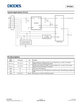
AP22953 Typical Applications Circuit CC Logic & Controller Uni-Directional ESD Protection Device Supply voltage from USB connector VBUS pin. Bypass VBUS_CON with a 1μF ceramic capacitor as close as possible to the device. Internal supply voltage rail to PMIC VBUS plane. Bypass VBUS_SYS with a 2.2μF ceramic capacitor as close as possible to the device. Enable Active-Low Input. Drive #EN low to enable the switch. Drive #EN high to disable the switch. Device ground. Connect to PCB ground plane
Open the catalog to page 2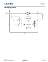
AP22953 Functional Block Diagram Logic Control
Open the catalog to page 3
AP22953 Absolute Maximum Ratings (@ TA = +25°C, unless otherwise specified.) Symbol HBM CDM Parameter Human Body Model ESD Protection Charged Device Model ESD Protection IEC 61000-4-2. Contact Discharge, VBUS_CON (Note 4) IEC 61000-4-2. Air Gap Discharge, VBUS_CON (Note 4) IEC 61000-4-5 Surge Protection, VBUS_CON (Note 4) Surge VBUS_CON Supply voltage from USB connector Internal supply DC voltage rail on the PCB Switch I/O Current (Continuous) Operating Ambient Temperature Storage Temperature Range Power Dissipation Thermal Resistance, Junction to Ambient Thermal Resistance, Junction to Case...
Open the catalog to page 4
AP22953 Electrical Characteristics (@ TA = +25°C, unless otherwise specified. CIN = 1μF, COUT = 2.2μF. Typical values are at VBUS = +5.0V, IVBUS ≤ 3.5A) (Note 6) Symbol Supply IVBUS_SLEEP VBUS_CON operating current consumption VBUS_CON operating current consumption Host mode leakage current Test Conditions (Note 7) VBUS_CON increasing from 5V VBUS_CON decreasing from 7V to 5V VBUS_CON decreasing from 7V to 5V VBUS_CON voltage rising from 0V to 5V Difference between rising and falling UVLO thresholds VBUS_CON voltage rising from 5V to 0V VBUS_SYS voltage rising from 0V to 5V Difference between...
Open the catalog to page 5
AP22953 Timing Diagrams (VBUS_CON = 5V, CIN = 1μF, CLOAD = 2.2μF, #EN = Enable, TA=25°C.) Thermal Shutdown VBUS_SYS tOFF_DELAY VOVP VBUS_CON tOVP_RES Figure 1. Timing for Power up, Normal operation, OTP and OVP protection
Open the catalog to page 6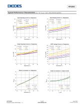
AP22953 Typical Performance Characteristics (CIN = 1µF, CLOAD = 2.2µF, unless otherwise specified.)
Open the catalog to page 7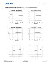
AP22953 Typical Performance Characteristics (CIN = 1µF, CLOAD = 2.2µF, unless otherwise specified.)
Open the catalog to page 8
AP22953 Typical Performance Characteristics (CIN = 1µF, CLOAD = 2.2µF, unless otherwise specified.) OVP Response Time CH1 = VBUS_CON, CH2 = VBUS_SYS, CH3 = #ACK VBUS_CON ramp from 5V to 10V
Open the catalog to page 9
Part Number Package Code 7” Tape and Reel Quantity Part Number Suffix XX : Identification Code Y : Year : 0~9 W : Week : A~Z : 1~26 week; a~ z : 27~52 week; z represents 52 and 53 week X : Internal Code Part Number Identification Code
Open the catalog to page 10
AP22953 Package Outline Dimensions Please see http://www.diodes.com/package-outlines.html for the latest version. (1) SEATING PLANE Suggested Pad Layout Please see http://www.diodes.com/package-outlines.html for the latest version. (1)
Open the catalog to page 11
IMPORTANT NOTICE 1. DIODES INCORPORATED AND ITS SUBSIDIARIES (“DIODES”) MAKE NO WARRANTY OF ANY KIND, EXPRESS OR IMPLIED, WITH REGARDS TO ANY INFORMATION CONTAINED IN THIS DOCUMENT, INCLUDING, BUT NOT LIMITED TO, THE IMPLIED WARRANTIES OF MERCHANTABILITY, FITNESS FOR A PARTICULAR PURPOSE OR NON-INFRINGEMENT OF THIRD PARTY INTELLECTUAL PROPERTY RIGHTS (AND THEIR EQUIVALENTS UNDER THE LAWS OF ANY JURISDICTION). 2. The Information contained herein is for informational purpose only and is provided only to illustrate the operation of Diodes products described herein and application examples. Diodes...
Open the catalog to page 12All Diodes Incorporated catalogs and technical brochures
 ZXCT21x
2 Pages
 ZXCT21x
15 Pages
 PI2MEQX2503
16 Pages
 AP43781
2 Pages
 APR3401
9 Pages
 AP3306
13 Pages
 AP3306
2 Pages
 AP43771H
9 Pages
 PAM8907
10 Pages
 PI6LC58S1101
17 Pages
 PI3EQX12902E
1 Page
 AP22653Q
13 Pages
 PAM8965
25 Pages
 Protection Products
2 Pages
 LOGIC PRODUCTS
20 Pages
 MOSFETS
20 Pages
 automotive products
20 Pages
 PRODUCT OVERVIEW
2 Pages
 Logic single gate 74AHC1G00
8 Pages
 AMR sensor angular ZMT32
10 Pages
 Audio amplifiers PAM8001
17 Pages
 Off-line LED drivers AL9910
15 Pages
 Operational amplifiers AP358
16 Pages
 Buck converter AP1501
12 Pages
 MOSFETs N Channel DMG1012T
6 Pages
 Bipolar transistor 2DA2018
5 Pages
 Schottky diodes 1N5711WS
3 Pages
 SENSORS AND MOTOR CONTROL
12 Pages
 LED Driver
16 Pages
 STANDARD LINEAR AND LOGIC
12 Pages
 Power Management
12 Pages
 BIPOLAR TRANSISTORS
24 Pages
 SBR®
SBR®12 Pages
 MOSFETs
16 Pages


Archived catalogs
 Diodes Product Design Guide
173 Pages

- Temperature probe
- Resistance temperature sensor
- Proximity switch
- Technology switch
- Signal amplifying integrated circuit
- Transceiver module
- Motor controller
- Rotary electric switch
- RTD temperature sensor
- Power amplifying integrated circuit
- DC motor controller
- Transistor module
- Touch switch
- Signal conditioner
- Magnetic proximity sensor
- Rectifier diode
- DC amplifier
- On/off switch
- Radio transceiver module