CVFD20065A
1 /6Pages

CVFD20065A
1 /6Pages
Catalog excerpts

Silicon Carbide Schottky Diode Z-Rec® Rectifier Features 650-Volt Schottky Rectifier Reduced VF for Improved Efficiency High Humidity Resistance Zero Forward and Reverse Recovery Voltage Temperature-Independent Switching Behavior Extremely Fast Switching Positive Temperature Coefficient on VF Replace Bipolar with Unipolar Rectifiers Essentially No Switching Losses Reduction of Heat Sink Requirements Parallel Devices Without Thermal Runaway Part Number Power Inverters Motor Drives EV Chargers Power Factor Correction Server Power Supplies Maximum Ratings (TC = 25 ˚C unless otherwise specified) Symbol Test Conditions Repetitive Peak Reverse Voltage Surge Peak Reverse Voltage DC Peak Blocking Voltage Continuous Forward Current Repetitive Peak Forward Surge Current TC=25˚C, tP=10 ms, Half Sine Pulse TC=110˚C, tP=10 ms, Half Sine Pulse Non-Repetitive Forward Surge Current TC=25˚C, tP=10 ms, Half Sine Pulse TC=110˚C, tP=10 ms, Half Sine Pulse Non-Repetitive Peak Forward Current Power Dissipation Operating Junction and Storage Temperature Nm M3 Screw lbf-in 6-32 Screw
Open the catalog to page 1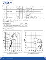
Electrical Characteristics Symbol VF Forward Voltage Total Capacitive Charge Total Capacitance Reverse Current Note: 1. This is a majority carrier diode, so there is no reverse recovery charge. Thermal Characteristics Symbol RθJC Thermal Resistance from Junction to Case Typical Performance Reverse Leakage Current, IRR (mA) IR (mA) Figure 1. Forward Characteristics Figure 2. Reverse Characteristics
Open the catalog to page 2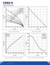
200 10% Duty 20% Duty 30% Duty 50% Duty 70% Duty DC Figure 3. Current Derating Conditions: TJ = 25 °C Ftest = 1 MHz Vtest = 25 mV Figure 4. Power Derating ReverseVR (V) VR (V) Voltage, Figure 5. Recovery Charge vs. Reverse Voltage Reverse Voltage, VR (V) VR (V) Figure 6. Capacitance vs. Reverse Voltage
Open the catalog to page 3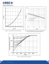
VR (V) Figure 7. Typical Capacitance Stored Energy Figure 8. Non-Repetitive Peak Forward Surge Current versus Pulse Duration (sinusoidal waveform) Thermal Thermal Resistance (oC/W) Resistance (˚C/W) Figure 9. Transient Thermal Impedance
Open the catalog to page 4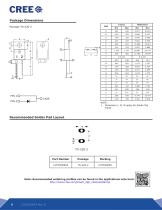
Package Dimensions Inches NOTE: 1. Dimension L, M, W apply for Solder Dip Finish Recommended Solder Pad Layout Part Number Note: Recommended soldering profiles can be found in the applications note here: http://www.cree.com/power_app_notes/soldering
Open the catalog to page 5
Diode Model Diode Model CSD04060 VfVfT = T + +If*RT T = V VT If*RT VTT= 0.965 + (Tj * -1.3*10-3) V = 1.0081+(TJ* -1.6*10-3) -3 RT = 0.0146+(TJ* 1.7*10-4) T= 0.096 + (Tj * 1.06*10 ) Note: Tj = Diode Junction Temperature In Degrees Celsius, valid from 25°C to 175°C Notes • RoHS Compliance The levels of RoHS restricted materials in this product are below the maximum concentration values (also referred to as the threshold limits) permitted for such substances, or are used in an exempted application, in accordance with EU Directive 2011/65/EC (RoHS2), as implemented January 2, 2013. RoHS Declarations...
Open the catalog to page 6All Cree catalogs and technical brochures
 Cree® XLamp® XP-G LEDs
27 Pages
 Cree® XLamp® XP-E2 LEDs
43 Pages
 Cree® XLamp® XR-C LEDs
25 Pages
 Cree® XLamp® XHP70.2 LEDs
31 Pages
 Cree® XLamp® XHP50.2 LEDs
30 Pages
 Cree® J Series® 2835 3‑V LEDs
54 Pages
 Cree® XLamp® XQ-E LEDs
30 Pages
 Cree® XLamp® XP-L2 LEDs
26 Pages
 Cree® LMD125 LED Module Drivers
12 Pages
 Cree® LMH2 LED Modules Family
20 Pages
 CLM1C Series White
10 Pages
 4-mm Oval LED Lamps C4SMA
10 Pages
 XQ Family Binning & Labeling
39 Pages
 Cree Edge Area/Flood Square
22 Pages
 304 Series Flood
8 Pages
 XSPW Wall Mount
3 Pages
 Cree Edge Security
6 Pages
 CGH80030D
5 Pages
 XLamp XP-L
35 Pages
 Cree ® XLamp ® XQ-A LEDs
19 Pages
 2015 LED LIGHTING CATALOG
172 Pages
 2016 LED LIGHTING PRODUCT GUIDE
24 Pages
 LMH2 LED Module
21 Pages
 XLamp ML-E
27 Pages
 304 Series Parking Structure
5 Pages
 CXB Series
2 Pages
 LED Lamps
28 Pages
 T8 Series
2 Pages
 CS Series
10 Pages
 CR24 UPKIT
1 Page
 UR Series LED Upgrade Kit
2 Pages
 SL Series
2 Pages
 WS Series
2 Pages
 LS Series
2 Pages
 XQ-B
XQ-B10 Pages
 XP-G2
XP-G213 Pages
 XP-G
XP-G12 Pages
 XP-E2
XP-E217 Pages
 XP-E High-Efficiency White
13 Pages
 XP-E
XP-E19 Pages
 XP-C
XP-C17 Pages
 XM-L2
XM-L212 Pages
 XM-L High-Voltage White
10 Pages
 XM-L
XM-L13 Pages
 XH-G
XH-G11 Pages
 XH-B
XH-B11 Pages
 XLamp XB-H LED
12 Pages
 XLamp XB-D LED
28 Pages
 MX-6S
MX-6S12 Pages
 XLamp ML-C
19 Pages
 XLamp ML-B
11 Pages
 XLamp Color LEDs
2 Pages
 LED Modules Product Guide
4 Pages
 Led light Catalog
156 Pages


Archived catalogs
 SMD LED Data Sheet
6 Pages
 Xlamp XR LED Data Sheet
13 Pages