- Catalogs
- CORNING Display Technologies
- Thin LCD Substrates Reduce Edge-Light Mura
Thin LCD Substrates Reduce Edge-Light Mura
1 /4Pages

Thin LCD Substrates Reduce Edge-Light Mura
1 /4Pages
Catalog excerpts

45.3: Thin LCD Substrates Reduce Edge-Light Mura Raymond G. Greene, Cynthia C. Contreras, Clive Gierbolini, Robert S. Schweiger, Corning Display Technologies, Corning Incorporated, Corning NY, USA Reducing LCD substrate thickness from 0.7 nun to 0.5 nun improves edge-light mura from glass thermal-stress birefringence by 26%. Sub nanometer (nm) resolution retardation mm thick substrates of width 4X2 mm and a height of305 nun with an LCD edge-light and are in good agreement with the stress The purpose of this paper is to quantify the effect of and to provide a model for the way thinner TFT/CF substrates improve the substrate contribution to edge-light mura on LCD displays. Figures 1 and 2 are CCD pictures of a commercial TN LC mode monitor and a commercial VA LC mode LCD-TV in black fields that show distinctive edge-light mura. These images were taken with a Radiant Imaging Inc. model PM-1423F camera. Figure 1. CCD picture of a TN LC mode monitor in black field shows distinctive edge-light mura. Figure 2. CCD picture of a VA LC mode LCD-TV in black field shows distinctive edge-light mura. A significant component of this mura is created by the stress in the panel glass due to the non-uniform temperature distribution from the heat of the edge/backlight. This stress creates distinctive smile-shaped retardation patterns on the edges of the glass. The TN polarizers at 457135° select die 0790° retardation component of thermal stress induced rctardancc as shown in Figure 1 as "H- band" mura on the edges. The VA polarizers at 0790° select the 457135° component of thermal stress induced retardance as shown in Figure 2 as "white corners". The experience of our lab is that, for typical LCD displays, the magnitude of this thermal stress-induced retardance can be of nm order. This is indeed significant compared to the black field panel retardance, typically on the order of a few nm's. Reference [1] gives a more detailed analysis of glass retardance effects on large LCD's. References [2] and [3] arc recent works about a system- level approach to these issues and analysis of the pressure sensitive adhesive (PSA) contributions to this issue. Figure 3 is a picture of our experimental setup. This consists of a vertical xy stage of approximately Gen 4 size and a Hinds Instruments custom-made retardance gage with generator and analyzer heads based on photo-elastic modulator (PEM) technology [4]. For these measurements, we use a 4 mm diameter spot of 633 nm wavelength to measure the retardance of the glass and an xy step size of 5 mm. Also shown are the edge-light and electronics from a commercial LCD monitor that is mounted to For these measurements we measured the various thicknesses of EAGLE XG® glass substrates with the edge-light off and on (warmed up) to be sure that the glass's intrinsic retardation was not significant. It should be noted that the 1.1 mm thick glass was Corning 1737 glass, not EAGLE XG. However, the precision of these measurements to the relevant material parameters of coefficient of thermal expansion (CTE), Young's modulus (E), and stress optic coefficient (SOC) arc not significantly different. It also should be noted that in a real LCD display, the edge-light is directly coupled to a typical PMMA waveguide behind the panel - not directly to the glass as in our setup. Nevertheless, we believe our configuration is representative and illustrative of the phenomena heat on the edge of the panel glass. 3. Physical Model of Thermal Stress Induced We start with the stress optic law [5] from the standard theory of photo elasticity with t as the thickness, R as the rctardancc, an as the first principal stress, and <7>2 as the second principal stress: Using Hooke's law, a = e * E, and e = CTE * AT, where AT is the temperature difference equation (1) becomes:
Open the catalog to page 1
SOC, E, and CTE for EAGLE XG glass are published in the publically available material data sheet. Their product is Figure 3. Kxperimental setup. Figures 4(a) and 4(b) give the total measured retardation magnitude for the edge-light in the off and on configurations for 1.1 mm thick glass cases respectively. The same intensity scale is used for both figures. These figures are representative of the results for the other measurements performed for edge-light in the 0.1 mm thicknesses. It should be noted that in our mounting configuration the right side of the glass was heat sunk to a vertical aluminum...
Open the catalog to page 2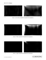
Figure 4. Total rctardancc magnitude: (a) edge-light off, (b) edge-light on. Figure 5. TN-filter transmission: (a) edge-light off, (b) edge-light on. Figure 6. VA-filtcr transmission: (a) edge-light off, (b) edge-light on.
Open the catalog to page 3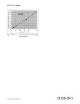
Figure 7. Maximum thermal stress retardance from edge-light
Open the catalog to page 4All CORNING Display Technologies catalogs and technical brochures
 Corning Iris®
2 Pages
 Aspheres by Corning
2 Pages
 UltraFlat™
2 Pages
 Tropel® FlatMaster® MSP
2 Pages
 Optical Solutions
4 Pages
 EAGLE XG® Slim
2 Pages
 Scoring of AMLCD Glass
4 Pages


Archived catalogs
 Gorilla® Glass 5
2 Pages
 Jade® Material Information Sheet
2 Pages
 Jade® Product Information Sheet
3 Pages


