- Catalogs
- Cirrus Logic
- WM0011
WM0011
1 /233Pages

WM0011
1 /233Pages
Catalog excerpts
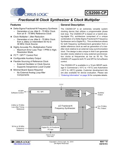
kTiTil iLiolfson microelectronics DESCRIPTION WM0011 Audio DSP provides Wolfson HD audio quality, with a power-budget targeted at handheld battery-powered audio devices. WM0011 combines the advanced Tensilica HiFi EP™ audio DSP with an I/O and peripheral set optimized for flexible integration into smartphones, tablets and other portable consumer electronics devices. WM0011 is ideal for extremely power-efficient implementations of advanced voice enhancement, telephony noise reduction, voice and music CODECs and general audio enhancement. A very wide range of audio CODECs, voice CODECs and third-party algorithms from such companies as Waves Audio, SRS Labs and Dolby are available, providing a rich portfolio of audio-processing options that can be integrated into a device with no additional software development. WM0011 comes in a space-saving 3x3mm 49-ball W-CSP package with 0.4mm pitch. APPLICATIONS • Wireless audio devices - headsets, microphones, speakerphones • Portable media devices • Automotive • General purpose digital signal processor for consumer audio applications • Smartphones FEATURES • 260MHz Tensilica HiFi EP™ 24-bit audio digital signal processor - C-programmable with advanced debugging and profiling tool set - 256kB local RAM memory - 36kB Instruction / Data cache memory - 384kB general-purpose system RAM - Flexible boot options with 32kB boot ROM - 32 Channel DMA - XTAL or CMOS clock input - Low-power programmable PLL • Security - Support for HW Authentication - Random Number Generator (RNG) to assist security algorithms • Peripherals - SPI Master / Slave interface - 3 x multi-channel AIF interfaces, including I2S and TDM - UART - I2C Master - I2C Slave - 3 x 32-bit general-purpose timer modules - Watchdog timer - On-chip JTAG debug unit and trace buffer - GPIO • Software-defined standby modes for extended battery life Production Data, August 2013, Rev 4.1 Copyright ©2013 Wolfson Microelectronics plc
Open the catalog to page 1
wolfson' microelectronics
Open the catalog to page 2
Production Data
Open the catalog to page 3
Production Data
Open the catalog to page 4
Production Data
Open the catalog to page 5
Production Data
Open the catalog to page 6
Production Data
Open the catalog to page 7
Production Data
Open the catalog to page 8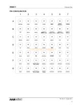
TDEBUG/ TMSDEBUG TMSDFT TDO TDI
Open the catalog to page 9
Production Data DEFAULT FUNCTION / RESET CONDITION (FUSES NOT PROGRAMMED) Pull-down enabled Pull-down enabled Pull-down enabled Pull-down enabled Pull-down enabled Pull-down enabled Pull-down enabled SPIMISO ¯¯¯¯¯ SPISS Pull-down enabled Pull-up enabled Pull-down enabled Pull-down enabled ¯¯¯¯¯¯ Pull-down enabled whilst RESET is asserted. Pull-down is disabled ¯¯¯¯¯¯ after RESET is released. UARTTX is then actively driven. Pull-down enabled Pull-down enabled Pull-down enabled Pull-down enabled Pull-down enabled Pull-down enabled ¯¯¯¯¯¯ Pull-down enabled whilst RESET is asserted. Pull-up is enabled...
Open the catalog to page 12
ABSOLUTE MAXIMUM RATINGS Absolute Maximum Ratings are stress ratings only. Permanent damage to the device may be caused by continuously operating at or beyond these limits. Device functional operating limits and guaranteed performance specifications are given under Electrical Characteristics at the test conditions specified. ESD Sensitive Device. This device is manufactured on a CMOS process. It is therefore generically susceptible to damage from excessive static voltages. Proper ESD precautions must be taken during handling and storage of this device. Wolfson tests its package types according...
Open the catalog to page 13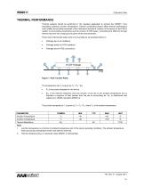
THERMAL PERFORMANCE Thermal analysis should be performed in the intended application to prevent the WM0011 from exceeding maximum junction temperature. Several contributing factors affect thermal performance most notably the physical properties of the mechanical enclosure, location of the device on the PCB in relation to surrounding components and the number of PCB layers. Connecting the GND pin through thermal vias and into a large ground plane will aid heat extraction. Three main heat transfer paths exist to surrounding air as illustrated below in: • Package top to air (radiation) • Package...
Open the catalog to page 14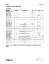
Selectable output drive strength control is provided on the digital output pads, using the *_DS register bits. The reduced drive strength option may be used at lower clock speeds, if preferred. Specific characteristic data for reduced drive strength is not available.
Open the catalog to page 15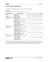
Typical power consumption data is provided below for a number of different operating conditions. Test Conditions: DCVDD = AVDD = 1.2V, DBVDD1 = 1.8V, DBVDD2 = DBVDD3 = 0V, Ta = +25°C The WM0011 supports a low-power Sleep mode, as referenced above. Note that, when the WM0011 is not in use, the Sleep mode (not the Reset mode) is recommended for typical applications. The Sleep mode allows the full processor functionality to be resumed at any time, without needing to re-load the software code. The Sleep mode also enables AIF Bypass modes to be selected.
Open the catalog to page 16
Table 2 System Clock and Phase Locked Loop (PLL) The WM0011 incorporates a 2-stage cascaded PLL circuit; the PLL timing parameters above refer to the 2-stage circuit in its entirety. Note that the specified frequency limits are not applicable to the internal reference points within the cascaded PLL circuits.
Open the catalog to page 17
AUDIO INTERFACE (AIF) TIMING DIGITAL AUDIO INTERFACE - MASTER MODE Figure 2 AIF Interface Timing - Master Mode Table 3 AIF Master Mode Timing Values Note the timing figures quoted in the table above are for full drive strength outputs; these timings are not guaranteed for reduced drive strength.
Open the catalog to page 18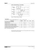
tLRH tLRSU Figure 3 AIF Interface Timing - Slave Mode Test Conditions DCVDD=AVDD=1.2V, DBVDD1=DBVDD2=DBVDD3=1.8V, Ta = +25°C, Cload=5pF (output pins) Table 4 AIF Slave Mode Timing Values Note the timing figures quoted in the table above are for full drive strength outputs; these timings are not guaranteed for reduced drive strength.
Open the catalog to page 19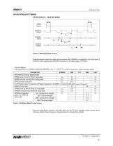
Note this diagram shows the mode where incoming data (SPIMISO) is sampled on the rising edge of SPISCLK, and outgoing data (SPIMOSI) transitions on the falling edge of SPISCLK. Test Conditions AVDD=DCVDD=1.2V, DBVDD1=DBVDD2=DBVDD3=1.8V, Ta = +25°C, Cload=5pF (output pins), unless otherwise stated. Table 5 SPI Master Mode Timing Values Note the timing figures quoted in the table above are for full drive strength outputs (except where otherwise stated); these timings are not guaranteed for reduced drive strength.
Open the catalog to page 20All Cirrus Logic catalogs and technical brochures


Archived catalogs
 CS48DV2/6
2 Pages
 Mixed-Signal Audio Brochure
64 Pages


- Bourn And Koch signal amplifier
- Bourn And Koch power amplifier
- Compact converter
- Serial converter
- Industrial converter
- Measuring amplifier
- Voltage amplifier
- Serial receiver
- Digital amplifier
- Power converter
- Bourn And Koch microcontroller
- Current amplifier
- Digital converter
- Isolated converter
- Digital receiver
- Analog converter
- Fast converter
- Audio amplifying integrated circuit
- Programmable converter
- Analog receiver