Catalog excerpts
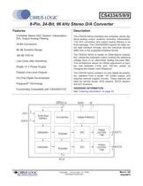
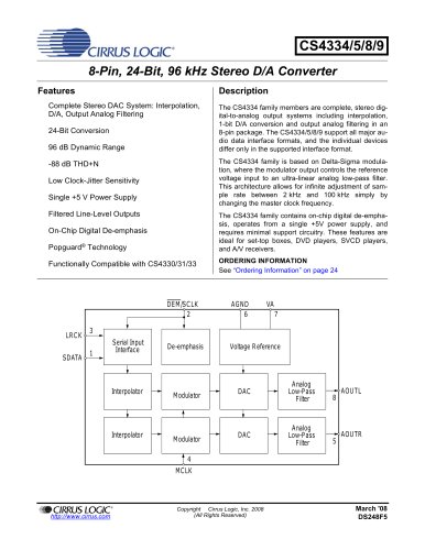
CS4334/5/8/9 8-Pin, 24-Bit, 96 kHz Stereo D/A Converter Features ♦ Complte Stereo DAC System: Interpolation, D/A, Output Analog Filtering ♦ 24-Bit Conversion ♦ 96 dB Dynamic Range ♦ -88 dB THD+N ♦ Low Clock-Jitter Sensitivity ♦ Single +5 V Power Supply ♦ Filtered Line-Level Outputs ♦ On-Chip Digital De-emphasis ♦ Popguard® Technology ♦ Functionally Compatible with CS4330/31/33 Description The CS4334 family members are complete, stereo dig-ital-to-analog output systems including interpolation, 1-bit D/A conversion and output analog filtering in an 8-pin package. The CS4334/5/8/9 support all major audio data interface formats, and the individual devices differ only in the supported interface format. The CS4334 family is based on Delta-Sigma modula譭tion, where the modulator output controls the reference voltage input to an ultra-linear analog low-pass filter. This architecture allows for infinite adjustment of sam-ple rate between 2 kHz and 100 kHz simply by changing the master clock frequency. The CS4334 family contains on-chip digital de-empha-sis, operates from a single +5V power supply, and requires minimal support circuitry. These features are ideal for set-top boxes, DVD players, SVCD players, and A/V receivers. ORDERING INFORMATION See "Ordering Information" on page 24 DEM/SCLK ,2 AGND VA ir7 LRCK-SDATA- 3 Serial Input Interface De-emphasis Voltage Reference 1 Interpolator AZ Modulator DAC Analog Low-Pass Filter AOUTL 8 Interpolator AZ Modulator DAC Analog Low-Pass Filter AOUTR 5 MCLK mCIRRUSLOGIC http://www.cirrus.com Copyright © Cirrus Logic, Inc. 2008 (All Rights Reserved) March '08 DS248F5
Open the catalog to page 1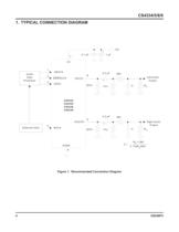
CS4334/5/8/9 1. TYPICAL CONNECTION DIAGRAM *-* +5V + 7 0.1 |jF 1jiF 1 -H VA SDATA DEM/SCLK AOUTL LRCK CS4334 CS4335 CS4338 CS4339 AOUTR MCLK AGND 8 3.3 jF 560 a Left Audio Output Audio Data Processor 2 -H 3 -H 267kQ. 10 ka C RL 5 3.3 jF 560 a 10 ka -> Right Audio Output RL 4 External Clock 267ka C C = R L + 560 4n Fs(RL560) 6 Figure 1. Recommended Connection Diagram 4 DS248F5
Open the catalog to page 4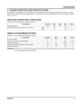
CS4334/5/8/9 2. CHARACTERISTICS AND SPECIFICATIONS (All Min/Max characteristics and spcifications are guaranteed over the Specified Operating Conditions. Typical performance characteristics and specifications are derived from measurements taken at nominal supply voltages and TA = 25°C.) SPECIFIED OPERATING CONDITIONS (AGND = 0V; all voltages with respect to ground.) Parameters Symbol Min Nom Max Units DC Power Supply VA 4.75 5.0 5.5 V Ambient Operating Temperature (Power Applied) -KSZ -DSZ Ta -10 - +70 -40 - +85 °C °C ABSOLUTE MAXIMUM RATINGS (AGND = 0V; all voltages with respect to...
Open the catalog to page 5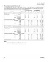
CS4334/5/8/9 ANALOG CHARACTERISTICS (Full-Scale Output Sine Wave, 997 Hz; Test load RL = 10 kQ, CL = 10 pF (see Figure 2). Fs for Base-Rate Mode = 48 kHz, Measurement Bandwidth 10 Hz to 20 kHz, unless otherwise specified; Fs for High-Rate Mode = 96 kHz, Measurement Bandwidth 10 Hz to 40 kHz, unless otherwise specified.) Base-Rate Mode High-Rate Mode Parameter Symbol Min Typ Max Min Typ Max Unit Dynamic Performance for CS4334/5/8/9-KSZ Dynamic Range (Note 1) 18 to 24-Bit 88 93 - - 90 - dB unweighted 91 96 - 91 96 - dB A-Weighted 86 91 - - 88 - dB 16-Bit unweighted 89 94 - 89 94 - dB...
Open the catalog to page 6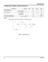
CS4334/5/8/9 POWER AND THERMAL CHARACTERISTICS Parameters Symbol Min Typ Max Units Power Supplies Power Supply Current normal opration Ia - 15 19 mA power-<Jown state 'a - 40 uA Power Dissipation (Note 7) normal opration - 75 104 mW power-down - 0,2 - mW Package Thermal R驩sistance 6ja - 110 - X/Watt Power Supply Rejection Ratio (1 kHz) PSRR - 79 - dB Notes: 7. Refer to Figure 4. Max Power Dissipation is measured at VA=5.5V 10 uF Figure 2. Output Test Load DS248F5
Open the catalog to page 8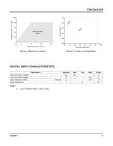
□RRUS LOGIC CS4334/5/8/9 125 Safe Operaling Rgion 10 15 Rsistive Load - Ri (kui 20 30 40 50 60 70 60 90 100 Sampie Rate (kHz) Figure 3. Maximum Loading Figure 4. Power vs. Sampie Rate DIGITAL INPUT CHARACTERISTICS Para met ers Symbol Min Typ Max Units High-Level Input Voltage V|H 2.0 驕 - V Low-Level Input Voltage v« - m 0.8 V Input Leakage Current (Note B) lil - - ±10 MA Input Capacrtance 8 - Notes: 8. Iin for CS433X LRCK is ±20pA max. DS248F5 9
Open the catalog to page 9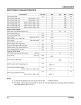
CS4334/5/8/9 SWITCHING CHARACTERISTICS Parameters Symbol Min Typ Max Units Input Sample Rate Fs 2 - 100 kHz MCLK Pulse Width High MCLK/LRCK = 512 10 - 1000 ns MCLK Pulse Width Low MCLK/LRCK = 512 10 - 1000 ns MCLK Pulse Width High MCLK / LRCK = 384 or 192 21 - 1000 ns MCLK Pulse Width Low MCLK / LRCK = 384 or 192 21 - 1000 ns MCLK Pulse Width High MCLK / LRCK = 256 or 128 31 - 1000 ns MCLK Pulse Width Low MCLK / LRCK = 256 or 128 31 - 1000 ns External SCLK Mode LRCK Duty Cycle (External SCLK only) 40 50 60 % SCLK Pulse Width Low tsclkl 20 - - ns SCLK Pulse Width High tsclkh 20 - - ns SCLK...
Open the catalog to page 10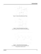
CS4334/5/8/9 LRCK SCLK SDATA Figure 5. External Serial Mode Input Timing LRCK SDATA *INTERNAL SCLK Figure 6. Internal Serial Mode Input Timing The SCLK puises shown are internai to the CS4334/5/8/9. *INTERNAL Figure 7. Internal Serial Clock Generation * The SCLK puises shown are internai to the CS4334/5/8/9. N equals MCLK divided by SCLK DS248F5 11
Open the catalog to page 11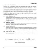
CS4334/5/8/9 3. GENERAL DESCRIPTION The CS4334 family of devices offers a complte stereo digital-to-analog system including digital interpolation, fourth-order delta-sigma digital-to-analog conversion, digital de-emphasis and analog filtering, as shown in Figure 8. This architecture provides a high tolerance to clock jitter. The primary purpose of using delta-sigma modulation techniques is to avoid the limitations of resistive laser trimmed digital-to-analog converter architectures by using an inherently linear 1 -bit digital-to-analog converter. The advan-tages of a 1-bit digital-to-analog...
Open the catalog to page 12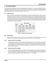
CS4334/5/8/9 4. SYSTEM DESIGN The CS4334 family accepts data at standard audio sample rates including 48, 44.1 and 32 kHz in BRM and 96, 88.2 and 64 kHz in HRM. Audio data is input via the serial data input pin (SDATA). The Left/Right Clock (LRCK) defines the channel and delineation of data, and the Serial Clock (SCLK) clocks audio data into the input data buffer. The CS4334/5/8/9 differ in serial data formats as shown in Figures 10-13. 4.1 Master Clock MCLK must be either 256x, 384x or 512x the desired input sample rate in BRM and either 128x or 192x the desired input sample rate in HRM....
Open the catalog to page 13All Cirrus Logic catalogs and technical brochures
-
Professional Service Partners
12 Pages
-
CS5343/44
21 Pages
-
WM0011
233 Pages
-
CS4970x4
31 Pages
-
CS4953xx
37 Pages
-
WM9081
103 Pages
-
CS42L51
84 Pages
-
CS42L42
184 Pages
-
CS43198
137 Pages
-
CS43131
156 Pages
-
CS43130
137 Pages
-
CS5351
23 Pages
-
CS5346
38 Pages
-
CS5341/42
21 Pages
-
CS35L32
51 Pages
-
CS35L00/01/03
34 Pages
-
Energy Measurement Brochure
13 Pages
Archived catalogs
-
CS48DV2/6
2 Pages
-
Mixed-Signal Audio Brochure
64 Pages

