video corpo

CS43198

CS43198
1 / 137 PagesView full catalog

CS43198

Product catalog summary
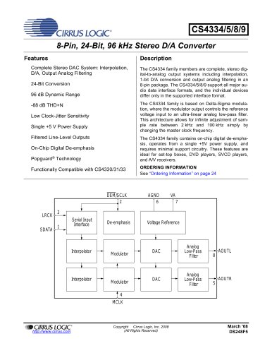
Overview: The CS43198 is a high-performance, 32-bit stereo audio DAC designed for high-resolution audio applications. It supports sampling frequencies up to 384 kHz and features pseudodifferential analog outputs. The DAC architecture includes a 32-bit oversampled multibit modulator with mismatch shaping technology to reduce distortion.
System Features:
  • Enhanced Delta-Sigma oversampling DAC architecture with 32-bit resolution and up to 384-kHz sampling rate.
  • Integrated high-performance outputs with 130-dB dynamic range and -115-dB THD+N.
  • Headphone detection with Popguard® technology to eliminate pop noise.
  • Integrated PLL supporting various system MCLK rates and providing clock output.
  • Support for Direct Stream Digital (DSD) path with up to 256•Fs DSD and patented DSD processor.
  • Serial audio input path with programmable Hi-Fi digital filter and multiple interface options.
Applications: The CS43198 is suitable for use in smartphones, tablets, portable media players, laptops, digital headphones, powered speakers, home theater systems, Blu-ray/DVD/SACD players, and professional audio equipment.
Functional Description: The DAC features proprietary digital-interpolation filters with selectable filter responses to minimize pre-echos and ringing artifacts. It includes volume control with 0.5-dB steps, wideband flatness mode support, and digital deemphasis for 44.1-kHz sample rate. The DSD processor allows for direct signal processing without intermediate decimation, preserving audio integrity.
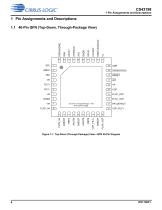
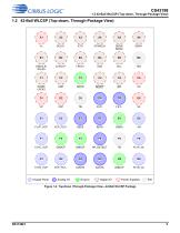
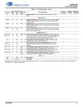
Pin Assignments and Descriptions: The document provides detailed pin assignments for both the 40-pin QFN and 42-ball WLCSP packages, including descriptions of each pin's function and internal connections.
Characteristics and Specifications: The document includes tables detailing parameter definitions, recommended operating conditions, absolute maximum ratings, and various output characteristics. It also covers digital interface specifications, power consumption, and switching characteristics.
PCB Layout Considerations: Recommendations for power supply, grounding, and routing are provided to ensure optimal performance and thermal management.
Performance Plots: The document includes plots illustrating digital filter responses and other performance metrics.
Package Dimensions and Thermal Characteristics: Detailed dimensions for the QFN and WLCSP packages are provided, along with thermal characteristics to guide proper implementation in designs.
Specifications and Test Conditions: The document outlines the analog output characteristics of the CS43198 under various test conditions. The test signal is a 32-bit, full-scale 997-Hz sine wave, with specific voltage and temperature settings. The performance data is collected with VA, VCP, VL, VD set to 1.8 V, VP to 3.6 V, and TA at +25°C. The measurement bandwidth is 20 Hz–20 kHz, and specific settings for ASP_SPRATE, PDN_XTAL, MCLK_INT, and MCLK_SRC_SEL are detailed.
PCM and DSD Processor Mode Parameters: The document provides minimum, typical, and maximum values for dynamic range and THD+N in both PCM and DSD modes. It specifies conditions such as RL, CL, DSD_SPEED, and DSD_DIRECT_GAIN, with dynamic range values ranging from 105 dB to 116 dB and THD+N values from -107 dB to -43 dB.
Wideband Flatness Mode: This section details the analog output characteristics in wideband flatness mode, with a focus on dynamic range, THD+N, idle channel noise, and full-scale output voltage. The dynamic range reaches up to 128 dB, and THD+N values are specified for different decibel levels.
Filter Characteristics: The document describes the DAC digital, on-chip analog, and AOUTx filter characteristics across different speed modes (Single, Double, Quad, and Octuple-Speed). It includes parameters like passband, stopband, group delay, and deemphasis error, with specific values for each mode.
DSD Combined Digital and On-Chip Analog Filter Response: This section provides details on the filter response in DSD processor mode and direct DSD mode, including passband, frequency response, and roll-off characteristics. The document specifies conditions such as DIR_DSD, DSD_SPEED, and DSD_DIRECT_GAIN, with frequency response values ranging from -0.67 dB to 0.06 dB.
Specifications: The frequency response is detailed for different modes, including Direct DSD Mode with low and high gain settings. The document specifies the passband to -0.1 dB and -3 dB corners in kHz. It also outlines the digital interface specifications, including input leakage current, internal weak pull-down resistance, and input capacitance.
Procedures: Test conditions are specified for various characteristics, including CLKOUT, PLL, and crystal characteristics. These conditions include voltage levels, temperature, and load capacitance.
Norms and Standards: The document adheres to specific electrical standards for logic levels, I2C interface timing, and power supply rejection ratio (PSRR) characteristics. It provides detailed tables for each parameter, including minimum, typical, and maximum values.
Recommendations: Recommendations are provided for power consumption in different use cases, such as off, standby, and playback modes. The document also suggests configurations for optimal performance, including clock/data line settings and power supply conditions.
Key Data from Tables: The tables provide critical data on frequency response, input leakage current, CLKOUT characteristics, PLL output frequency, crystal oscillator frequency, and power consumption. For example, the PLL output frequency ranges from 22.5792 MHz to 24.576 MHz, and the power consumption in standby mode is 576 µW.
Functional Description: The document includes a functional description section that outlines the general theory of operation of the CS43198. It covers signal and control flow through various blocks within the device, including analog outputs, class H output, headphone presence detect, clocking architecture, and filtering options.
Analog Outputs: The analog output block provides pseudodifferential outputs with adaptable full-scale voltage settings. The digital volume control allows for independent signal level adjustments in 1/2 dB increments. The CS43198 supports mono mode playback and wideband flatness mode for optimized audio performance.
Class H Output: The CS43198 utilizes Class H technology to optimize power efficiency by adjusting rail voltages based on the output signal level. It offers standard Class AB operation and adapt-to-output signal mode, with power-supply transitions managed by an internal charge pump.
Headphone Detection: The device can detect headphone presence and notify the application processor via an interrupt event.
Audio Interfaces and Supported Formats: The CS43198 features two serial input ports, ASP and XSP, supporting various audio formats. It also includes a DSD interface for high-quality audio streaming.
System Clocking: The internal MCLK can be sourced from multiple options, providing flexibility for different audio applications. The clock output supports high-quality audio rate system clocks.
System Interrupts and Reset: The device includes an open-drain interrupt output and offers two types of reset options: asserting RESET and power-on reset (POR).
Power Down: The CS43198 allows for powering down individual components, with specific sequences required to avoid entering an unresponsive state.
Power Supply Control Options: The device supports standard Class AB operation and adapt-to-output signal mode, with specific settings for rail voltages and power-supply transitions.
External VCP_FILT Power-Up and Power-Down Sequences: For powering up the CS43198 in external VCP_FILT mode, follow these steps: set EXT_VCPFILT and HV_EN bits, wait 8 ms after I2C ACK, release and ramp external voltage on VCP_FILT± pins, wait until VCP_FILT+ is greater than +2.6V and VCP_FILT– is less than –2.6V, then clear the PDN_HP bit. For powering down, set PDN_HP, wait 8 ms after I2C ACK, shut off external supply to VCP_FILT± pins, wait for Hi-Z mode on VCP_FILT± pins, and clear EXT_VCPFILT and HV_EN bits.
Headphone Presence Detect: The CS43198 supports headphone presence-detect functionality via the HP_DETECT sense pin, which is debounced to filter out brief events. The presence detect function uses a small current source to pull up the pin if no plug is inserted. Various registers control the debounce times and interrupt statuses for plug and unplug events.
Clocking Architecture: The CS43198 requires a Master Clock (MCLK) for operation, which can be sourced from a crystal oscillator, externally through the XTI/MCLK pin, or using an internal RC oscillator. The device supports switching between clock sources, but care must be taken to ensure the new source is ready before switching to avoid non-responsive states.
Clock Output and Fractional-N PLL: The CS43198 includes a fractional-N PLL to support various clocking requirements. The PLL can be configured using several registers to set the reference clock, output frequency, and other parameters. Powering up and down the PLL involves specific sequences to ensure proper operation.
Filtering Options: The CS43198 offers selectable filters for different playback modes, including fast and slow roll-off interpolation filters, low-latency options, and a nonoversampling mode. In DSD processor mode, features like matched PCM level output and DSD volume control are available.
Audio Serial Port (ASP): The CS43198 features configurable ASPs and auxiliary serial ports (XSPs) for audio data communication. These ports support common audio interfaces and can operate in master or slave timing modes, with specific configurations for PCM and DoP stream playback.
Audio Serial Port (ASP) Configuration:
  • Sample Rate and Bit Size: The serial port sample rate register (xSP_SPRATE) and sample bit size register (ASP_SPSIZE or XSP_SPSIZE) must be configured according to the audio content before enabling the serial port for both PCM and DoP playback.
  • Power Management: The xSP has separate power-down (PDN_xSP) and tristate (xSP_3ST) controls to minimize power consumption when the input port is not in use. Master/slave operation is controlled by the xSP_M/S setting.
  • I/O Configuration: The ASP and XSP ports are associated with specific pins (SDIN, SCLK, LRCK) and can be configured for high-impedance mode to allow multiple masters on a clock bus without external buffers.
  • Clock Generation: The CS43198 provides flexible clock generation for independent clocking of serial ports, with configurable SCLK and LRCK/FSYNC signals. Polarity controls for SCLK and LRCK are available to adjust signal timing.
  • Channel Configuration: Each serial-port channel has programmable location and size, ensuring data does not extend beyond frame boundaries.
  • Frame Start Phase: The frame start phase can be configured to begin when LRCK/FSYNC is high or low, depending on the xSP_STP setting.
  • 50/50 Mode: In two-channel I2S operation, the LRCK duty cycle is 50%, with each channel transferred during one of the two LRCK phases.
  • Status and Control: Each serial port has status bits for monitoring errors and clock pin states, with mask bits to control interrupt settings.
DoP (DSD over PCM) Mode:
  • DoP Protocol: DoP is used for packetizing DSD data into PCM frames for transmission over I2S interfaces. The ASP or XSP can accept DSD data in DoP format.
  • Configuration: To enable DoP, configure the ASP according to DoP content requirements, set DSD_SPEED, and enable DSD processing with DSD_PRC_SRC and DSD_EN settings.
Programmable Filter: The CS43198 features programmable filters that allow users to customize frequency response. These filters include one first-order IIR system and three second-order IIR systems, forming a seventh-order system. Filters can be programmed via I2C writes to specific register addresses and should be disabled in certain modes like WBF and impedance measurement.
Applications: The document outlines procedures for standard operations of the CS43198, including PLL clocking, power sequencing, and crystal tuning. The PLL is necessary when the external MCLK is not 22.5792 or 24.576 MHz. Power sequencing requires VP to be powered first and last during power-up and power-down, respectively.
Crystal Tuning: The CS43198 uses an external crystal for MCLK. The document provides a formula for calculating the oscillation frequency and lists supported crystals with their settings. Proper tuning involves selecting appropriate load capacitors and verifying communication with the CS43198.
Analog Output and Filtering: An external opamp filter stage is required for driving headphone loads. The document emphasizes that the DAC system's phase response depends on external circuitry.
Power Down and Up Sequences: Detailed sequences for powering down and up the audio output in PCM and DSD modes are provided. These sequences ensure proper shutdown and startup without audible pops.
Enabling and Disabling NOS Filter: The document describes sequences for enabling and disabling the NOS filter, ensuring pop-free transitions.
PCM Invert Bits: Instructions for enabling and disabling PCM invert bits for channels A and B are included, allowing for channel inversion as needed.
PCM Channel Operations:
  • Channel Inversion: Procedures for enabling and disabling inversion on channels A and B are outlined, involving specific register manipulations (e.g., 0x90004 data).
  • Channel Swap: Steps to enable and disable PCM channel swapping are provided, including register settings to control the PCM_SWAP_CHAN bit.
Mono Mode for PCM Playback:
  • Enabling/Disabling Mono Mode: Detailed sequences for toggling mono mode are described, with specific register values to be set for enabling and disabling this mode.
Example Sequences:
  • Power-up to I2S Playback: A comprehensive sequence is provided for initializing the system to I2S playback, including power supply application, XTAL configuration, ASP interface setup, and DAC output configuration.
  • Power-up to DSD Playback: Instructions for setting up DSD playback are detailed, covering PLL configuration, DSD interface setup, and DAC output adjustments.
Key Configurations:
  • XTAL and PLL Settings: Specific register settings for XTAL and PLL configurations are highlighted, crucial for clock management and synchronization.
  • ASP and DSD Interface: Configuration steps for ASP and DSD interfaces are provided, ensuring proper data handling and playback quality.
Interrupt Management:
  • Instructions for enabling and managing various interrupts, including XTAL, PLL, and headphone detection, are included to ensure robust system operation.
Power-Up Sequences:
  • DoP Playback with PLL: Involves configuring the PLL, setting predivide and output divide values, and enabling PLL interrupts. The ASP interface is configured for DoP input with a sample rate of 176.4 kHz.
  • I2S Playback in Mono Mode: Utilizes a 22.5792-MHz crystal, with ASP set as I2S master at 44.1 kHz. The sequence includes enabling ASP clocks and configuring the PCM interface.
  • DSD Playback in Mono Mode: Uses a PLL to create a 24.576-MHz MCLK, with XSP set as DSD slave at 2.8224 MHz.
Procedures:
  • Detailed steps for configuring registers and bit fields for each playback mode are provided, including tasks like setting PLL calibration ratios, enabling interrupts, and configuring ASP and DSD interfaces.
  • Instructions for setting DAC output to full scale and configuring Class H amplifiers are included.
Interrupt Configuration:
  • Interrupts for various functions such as PLL readiness, headphone detection, and ASP errors are configured and enabled as part of the setup sequences.
Recommendations:
  • Ensure all relevant power supplies are applied and reset is asserted before starting configuration sequences.
  • Follow the specified wait times between steps to ensure proper initialization and operation.
Interrupt Configuration:
  • Various interrupts are enabled or disabled to manage different operational states, such as DSD_STUCK, DSD_INVAL, DSD_SILENCE, and DOP_MRK_DET.
  • Specific interrupts are masked or unmasked to handle events like headphone detection and XTAL readiness.
DoP Playback with PLL in Mono Mode:
  • Steps include waiting for PLL readiness, setting MCLK source and frequency, enabling ASP clocks, and powering up the DAC.
  • Configuration involves setting MCLK to 22.5792 MHz and using PLL as the source.
Switching MCLK Frequency:
  • Instructions for changing MCLK frequency to accommodate different audio sample rates.
  • Involves switching MCLK source to RCO, setting new frequency, and configuring ASP for the new sample rate.
Headphone Detection:
  • Sequence for detecting headphone presence, including enabling HPDETECT interrupts and configuring debounce times.
  • Involves reading and clearing interrupt status registers.
DoP and PCM Mixing:
  • Detailed steps for mixing DoP and PCM signals, including configuring XTAL, XSP, and ASP interfaces.
  • Involves setting sample rates, bit sizes, and enabling necessary interrupts for seamless operation.
Configuration Details:
  • Registers and bit fields are specified for each task, providing precise control over the audio codec's operation.
  • Includes power-up sequences, clock configurations, and signal path controls for both DSD and PCM paths.
Conclusion: The document serves as a comprehensive guide for configuring the CS43198 codec in various audio processing scenarios, emphasizing the importance of precise register settings and interrupt management.
Global Registers:
  • Device ID and Revision: The device ID and revision levels are specified, with alpha and metal revision levels forming the complete device revision ID.
  • System Clocking Control: Configures the internal MCLK frequency and source selection, with options for direct MCLK/XTAL mode, PLL mode, and RCO mode.
  • Serial Port Sample Rate: Defines the ASP sample rate, which must be programmed for both Master and Slave modes. The default rate is 44.1 kHz, with options ranging from 32 kHz to 384 kHz.
  • Power Down Control: Manages power states for various components, including XSP, ASP, DSD interface, and PLL, with default settings powering down most components.
PLL Registers:
  • PLL Settings: Includes multiple settings for configuring the PLL, such as start bit, fractional and integer portions of the divide ratio, and calibration ratio. The PLL can be started after proper configuration.
ASP and XSP Registers:
  • Clock Configuration: Configures the clock output and source selection for CLKOUT, with options for dividing the internal MCLK path.
  • Sample Rate and Bit Size: Defines the sample rate and bit size for ASP and XSP, with default settings for 24-bit size and various sample rates.
  • Frame Configuration: Controls the start phase and duty cycle of the LRCK/FSYNC, with options for programmable or fixed 50% duty cycle.
Key Parameters and Recommendations:
  • Ensure proper configuration of PLL settings before enabling the PLL output.
  • Power down associated serial ports before changing certain register values to avoid conflicts.
  • Use default settings as a baseline and adjust according to specific application requirements.
ASP and XSP Channel Configuration: The document outlines the configuration settings for ASP and XSP channels, including their location, size, and enable settings. Each channel can be set to start at different SCLK periods within a TDM frame, with default starting at SCLK 0. The channels can be enabled or disabled, and their resolution can be set to 8, 16, 24, or 32 bits per sample, with 24 bits as the default.
DSD Registers: The DSD registers control various aspects of the DSD processor, including volume control, signal path, and interface configuration. Volume can be adjusted in 0.5 dB increments, with a default setting of -60 dB. The DSD processor supports features like soft volume ramp-up, auto mute, and phase modulation. The document also details the configuration for mixing PCM and DSD streams.
Analog Output and PCM Registers: The analog output section includes settings for output full scale voltage, which can be set to 1.41 V or 1.73 V, with an option to increase to 2 V under certain conditions. PCM filter options include fast and slow filters, phase-compensated filters, and non-oversampling emulation mode. PCM volume control is similar to DSD, allowing independent control in 0.5 dB increments. The PCM path signal control includes options for soft ramp, auto mute, and channel swapping.
Programmable Filter Control: The document concludes with programmable filter controls, allowing enabling or disabling of SOS and FOS filters. Each filter has specific control bits to manage its operation.
Programmable Filter Control: Address 0x9 000B allows control over SOS1, SOS2, and FOS coefficients via the control port. Each coefficient can be enabled or disabled, with a default setting of disabled (0). When the filter is not in use, these bits must be cleared to 0.
Programmable Filter Coefficients: Addresses 0x9000C–0x90041 detail the programmable filter coefficients, which are formatted in Q1.17. Refer to Section 4.13 for more details.
Class H Control: Address 0xB0000 manages adaptive power adjustment, high voltage mode, and external VCP_FILT± voltage mode. The default setting adapts power to the signal, with high voltage mode enabled.
HP Detect: Address 0xD0000 configures the headphone detect circuit, including control, inversion, and debounce times for rising and falling signals. The default setting disables the HP detect circuit.
HP Status: Address 0xD0001 provides status on HP plug and unplug debounce conditions, with default settings indicating no conditions present.
Interrupt Status and Mask Registers: Various addresses (0xF0000 to 0xF0014) provide status and mask settings for different interrupt conditions, including DAC overflow, HP detect events, XTAL and PLL conditions, ASP and XSP errors, and DSD conditions. Default settings generally mask these interrupts.
PCB Layout Considerations: Guidelines for PCB layout emphasize careful power supply and grounding arrangements, use of decoupling capacitors, and proper routing of REFA and REFB for optimal performance. The QFN package requires a thermal pad connection to ground for heat dissipation.
Performance Plots: Digital filter responses are illustrated with plots showing passband ripple, stopband attenuation, and impulse and step responses for both slow and fast roll-off at a single speed (Fs = 32 kHz).
Digital Filter Response: The document details various digital filter responses for the CS43198 DAC, including single, double, quad, and octuple speed modes with both slow and fast roll-off characteristics. Key figures illustrate passband ripple, stopband attenuation, impulse response, and step response for each mode.
Package Dimensions: The document provides dimensions for the 40-Pin QFN and 42-Ball WLCSP packages, including total thickness, lead width, and body size, with tolerances specified per ASME standards.
Thermal Characteristics: Thermal resistance parameters are provided for typical JEDEC four-layer boards, including junction-to-ambient, junction-to-board, and junction-to-case thermal resistances.
Ordering Information: The CS43198 DAC is available in 42-ball WLCSP and 40-pin QFN packages, with commercial temperature ranges and RoHS compliance. Specific order numbers are provided for different packaging options.
References and Revision History: The document references the I2C-Bus Specification and User Manual by NXP Semiconductors and includes a revision history noting the initial release in October 2017.
Disclaimer and Usage Restrictions: The document outlines that Cirrus Logic products are not designed or warranted for use in critical applications such as life support, automotive safety, or nuclear systems. Any use in such applications is at the customer's risk, and Cirrus Logic disclaims all warranties, including implied warranties of merchantability and fitness for a particular purpose. Customers using these products in critical applications agree to indemnify Cirrus Logic from any resulting liabilities.
Intellectual Property and Reproduction Rights: The document is the property of Cirrus Logic and does not grant any license under intellectual property rights. Reproduction of the document is allowed only within the organization for use with Cirrus Logic products, without alteration and with all notices intact. This consent does not extend to general distribution or promotional purposes.
Warranty Disclaimer: The information is provided "AS IS" without any express or implied warranty. Cirrus Logic assumes no responsibility for the use of the information, including any potential patent infringement.
Trademarks: Cirrus Logic, the Cirrus Logic logo, and SoundClear are trademarks of Cirrus Logic. DSD and DSD Direct Stream Digital are registered trademarks of Sony Corporation.
Copyright: © 2015–2017 Cirrus Logic, Inc. All rights reserved.
See more

Catalog excerpts

CS43198-1

CS43198 130-dB, 32-Bit High-Performance DAC with Pseudodifferential Outputs System Features Applications • Smart phones, tablets, portable media players, laptops, digital headphones, powered speakers, AVR, home theater systems, Blu-ray/DVD/SACD players, and pro audio TSO Interrupt Sources XSP/DSD Audio Interface AOUTB REFB FLYC_VCP FLYP_VCP FLYN_VCP VCP_FILT+ VCP_FILTFLYP_VA FLYN_VA -VA Interpolation Filter and Volume Control Register/Hardware Configuration DSD Processor Popguard® Circuitry Control Port Level Translator Copyright  Cirrus Logic, Inc. 2015–2017 (All Rights Reserved) Charge Pump Internal Voltage Reference Interpolation Filter and Volume Control Analog Supply (VA,VCP) Battery Supply +1.8V (VP) FILT+ FILT- Digital LDOs Digital Core Internal Interface Supply (VL) Supply (VD) +1.8V +1.8V Level Translator • Direct Stream Digital (DSD®) path — Up to 256•Fs DSD Enhanced  oversampling DAC architecture — Patented DSD processor — 32-bit resolution – On-chip 50-kHz filter to meet Scarlet Book Super — Up to 384-kHz sampling rate Audio Compact Disk (SACD) recommendations — Low clock jitter sensitivity – Matched PCM and DSD analog output levels — Auto mute detection – Nondecimating volume control with 0.5-dB step size Integrated high performance outputs and soft ramp — 130-dB dynamic range (A-weighted) – DSD and Pulse-code modulation (PCM) mixing for — –115-dB total harmonic distortion + noise (THD+N) alerts — 110-dB interchannel isolation — Dedicated DSD and DoP pin interface — Up to 2-Vrms pseudodifferential stereo analog output • Direct DSD path support Headphone detection • Serial audio input path — Headphone plug-in detection — Programmable Hi-Fi digital filter — Popguard® technology eliminates pop noise — Five selectable digital filter responses Integrated PLL – Low-latency Mode minimizes pre-echo — Support for 11.2896-/22.5792-, 12.288-/24.576-, 9.6-/ – 110 dB of stopband attenuation 19.2-, 12-/24-, and 13-/26-MHz system MCLK rates — Supports sample rates from 32 to 384 kHz — Reference clock sourced from XTI/MCLK pin — I2S, right-justified, left-justified, TDM, and — System clock output DSD-over-PCM (DoP) interface Mono Mode (differential) support — Master or slave operation I2C control—up to 1 MHz — Volume control with 0.5-dB step size and soft ramp — 44.1 kHz deemphasis and inverting feat

 Open the catalog to page 1
CS43198-2

CS43198 General Description The CS43198 is a high-performance, 32-bit resolution, stereo audio DAC that supports up to 384-kHz sampling frequency with pseudodifferential analog outputs. The advanced 32-bit oversampled multibit modulator with mismatch shaping technology eliminates distortion due to on-chip component mismatch. Proprietary digital-interpolation filters support five selectable filter responses with pseudo-linear phase and ultralow latency to minimize pre-echos and ringing artifacts. An on-chip programmable filter is available for further response customization. Other features include...

 Open the catalog to page 2
CS43198-3

CS43198 Table of Contents 1 Pin Assignments and Descriptions . . . . . . . . . . . . . . . . . . . . . . 4 1.1 40-Pin QFN (Top-Down, Through-Package View) . . . . . . . . . 4 1.2 42-Ball WLCSP (Top-down, Through-Package View) . . . . . . 5 1.3 Pin Descriptions . . . . . . . . . . . . . . . . . . . . . . . . . . . . . . . . . . . 6 1.4 Electrostatic Discharge (ESD) Protection Circuitry . . . . . . . . 8 2 Typical Connection Diagram . . . . . . . . . . . . . . . . . . . . . . . . . . 10 3 Characteristics and Specifications . . . . . . . . . . . . . . . . . . . . . 12 Table 3-1. Parameter Definitions...

 Open the catalog to page 3
CS43198-4

CIRRUS LOGIC CS43198 1 Pin Assignments and Descriptions 1 Pin Assignments and Descriptions 1.1 40-Pin QFN (Top-Down, Through-Package View) Q w < Q W Q RESET TNT VP VCP FLYP_VCP FLYC_VCP HP_DETECT VCP FILT+ Figure 1-1. Top-Down (Through-Package) View—QFN 40-Pin Diagram

 Open the catalog to page 4
CS43198-5

1.2 42-Ball WLCSP (Top-down, Through-Package View) 1.2 42-Ball WLCSP (Top-down, Through-Package View) Charge Pump Power Supplies Figure 1-2. Top-Down (Through-Package) View—42-Ball WLCSP Package

 Open the catalog to page 5
CS43198-7

I.The power supply is determined by ADPT_PWR setting (see Section 4.3.1). VP is used if ADPT_PWR = 001 (VP_LDO Mode) or when necessary for ADPTPWR = 111 (Adapt-to-Signal Mode).

 Open the catalog to page 7
CS43198-8

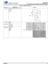
1.4 Electrostatic Discharge (ESD) Protection Circuitry 1.4 Electrostatic Discharge (ESD) Protection Circuitry ESD-sensitive device. The CS43198 is manufactured on a CMOS process. Therefore, it is generically susceptible to damage from excessive static voltages. Proper ESD precautions must be taken while handling and storing this device. This device is qualified to current JEDEC ESD standards. Fig. 1-3 provides a composite view of the ESD domains showing the ESD protection paths between each pad and the substrate (GND), as well as the interrelations between some domains. Note that this figure...

 Open the catalog to page 8
CS43198-9

1.4 Electrostatic Discharge (ESD) Protection Circuitry Table 1-2. ESD Domains (Cont.) ESD Domain VA/–VA Signal Name (See * in Topology Figures for Pad) FLYN_VA FLYP_VA FILT+ FILT– RESET INT VP/VCP_FILT– FLYP_VCP FLYC_VCP HP_DETECT VCP_FILT+/ FLYN_VCP VCP_FILT– AOUTA AOUTB REFA REFB VP/GNDCP Domain VCP_FILT+/VCP_FILT– Domain VP/VCP_FILT– Domain

 Open the catalog to page 9
CS43198-10

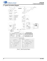
2 Typical Connection Diagram 2 Typical Connection Diagram VL DoP / DSD Digital Audio Source PCM / DoP Digital Audio Source Audio Devices OUTB AOUTA Applications Processor / MicroController Analog Signal Conditioning All external passive component values shown are nominal . Clocking Configuration XTAL External MCLK System Clock REFB RESET Headphone Connector Key for Capacitor Types Required : * Use low ESR, X7R/X5R capacitors If no type symbol is shown next to a capacitor, any type may be used. ** Use C0G capacitors. XTI/MCLK XTI/MCLK VCP_FILT Configuration EXT_VCPFILT = 0 VCP VCP_FILT+ VCP_FILT–...

 Open the catalog to page 10
*Prices are pre-tax. They exclude delivery charges and customs duties and do not include additional charges for installation or activation options. Prices are indicative only and may vary by country, with changes to the cost of raw materials and exchange rates.