video corpo

CS43131

CS43131
1 / 156 PagesView full catalog

CS43131

Product catalog summary
Overview: The CS43131 is a high-performance, 32-bit stereo audio DAC designed for high-quality audio output applications. It supports sampling frequencies up to 384 kHz and includes low-noise, ground-centered headphone amplifiers.
Key Features:
  • DAC Architecture: Utilizes a 32-bit oversampled multibit modulator with mismatch shaping technology to reduce distortion.
  • Headphone Amplifiers: Delivers over 30 mW into a 32-Ω load or 5 mW into a 600-Ω load per channel, with a maximum output of 2 Vrms on a 600-Ω load.
  • Impedance Detection: Proprietary headphone impedance detection for enhanced digital post-processing.
  • DSD Processor: Includes a patented on-chip DSD processor for direct signal processing without intermediate decimation.
  • Audio Interfaces: Supports I2S, right-justified, left-justified, and TDM-format PCM data, with sample rates from 32 to 384 kHz.
  • Control Interface: Configurable via a high-speed I2C interface capable of up to 1 MHz operation.
  • Clocking Flexibility: Integrated PLL for flexible clocking and Popguard® technology to eliminate output transients.
Applications: Suitable for smartphones, tablets, portable media players, laptops, digital headphones, powered speakers, AVR, home theater systems, Blu-ray/DVD/SACD players, and professional audio equipment.
Specifications:
  • Dynamic Range: 130 dB (A-weighted)
  • THD+N: -115 dB
  • Interchannel Isolation: 110 dB
  • Package Options: Available in 42-ball WLCSP or 40-pin QFN packages.
Functional Description: The CS43131 features advanced digital-interpolation filters with selectable responses, volume control with 0.5-dB steps, and wideband flatness mode support. It includes an internal stereo audio switch for alternate analog input paths, reducing material costs and PCB area.
Performance and Design Considerations: Detailed specifications, pin assignments, connection diagrams, and layout considerations are provided to optimize performance and integration into various systems.
Specifications Overview: Detailed specifications focus on analog output characteristics under various conditions, including idle channel noise, full-scale output voltage, output power, interchannel isolation, and THD+N.
Analog Output Characteristics:
  • HV_EN = 1: Idle channel noise at 0.55 µV, full-scale output voltage from 4.66 Vpp to 5.14 Vpp, output power typically 5 mW, interchannel isolation 120 dB at 217 Hz and 1 kHz, THD+N at -105 dB.
  • HV_EN = 0: Idle channel noise at 0.55 µV, full-scale output voltage from 3.76 Vpp to 4.16 Vpp, output power typically 3.3 mW, consistent interchannel isolation, dynamic range up to 128 dB for 24-bit, 32-bit A-weighted.
Wideband Flatness Mode: Dynamic range at 128 dB A-weighted for 24-bit, 32-bit formats, THD+N from -112 dB to -106 dB, idle channel noise at 0.69 µV.
Headphone Load Measurement: Frequency range 20 Hz to 20 kHz, impedance measurement accuracy includes a gain error of ±10% and an offset of ±1 Ω.
Alternate Headphone Path: Signal range up to 3.00 Vpp, THD+N with a 32 Ω load at 2.82 Vpp is -103 dB, interchannel isolation at 110 dB at 1 kHz.
Additional Characteristics: Minimal interchannel gain and phase mismatches, output offset voltage during mute is ±50 to ±100 µV, gain drift is ±100 ppm/°C, load resistance and capacitance specified for various configurations, turn-on time is 12 ms, audio latency after reset is 22 ms, click/pop noise during power enable/disable is ±50 to ±100 µV.
Filter Characteristics: Outlines filter characteristics for various modes: Single-Speed, Double-Speed, Quad-Speed, and Octuple-Speed, with Fast Roll-Off and Slow Roll-Off filters described.
Digital Interface Specifications: Specifications for input leakage current, internal weak pull-down, input capacitance, and logic levels for both non-I2C and I2C modes.
Clock and PLL Characteristics: Details on CLKOUT output frequency, duty cycle, and jitter, PLL characteristics such as output frequency, lock time, and reference clock input.
Crystal and Power Supply Characteristics: Crystal oscillator frequency, load capacitance, and startup time outlined, Power Supply Rejection Ratio (PSRR) measured under various conditions.
DC Characteristics and Power Consumption: DC characteristics include VCP_FILT voltages, on-resistance, and power-on reset thresholds, power consumption detailed under specific test conditions.
Conclusion: Comprehensive technical data necessary for understanding the performance and integration of the CS43131 DAC in audio applications, emphasizing its filter characteristics, digital interface, and power management capabilities.
Power Modes and Use Cases: Outlines different power configurations such as Off, Standby, and Playback modes, detailing typical current consumption and power usage.
Serial-Port Interface Characteristics: Describes timing and frequency characteristics of the serial port interfaces in both Master and Slave modes.
DSD Switching Characteristics: Specifies DSD clock and data timing, including duty cycles and pulse widths for different oversampling rates.
I2C Slave Port Characteristics: Details on the I2C interface include clock frequency, setup and hold times, and bus capacitance.
Functional Description: Explains the operation of the CS43131, covering analog outputs, headphone detection, and system clocking.
System Clocking and Interrupts: The CS43131 can source its internal MCLK from direct, PLL, or RCO modes, with specific configurations for each.
Power Management: Describes power-down procedures and reset options, emphasizing the importance of following specific sequences to avoid unresponsive states.
Analog Outputs Overview: Provides analog outputs derived from digital audio inputs, outlining the signal flow and control mechanisms.
Analog Output Signal Flow: Features four full-scale voltage settings controlled by OUT_FS[1:0], digital volume control allows for independent signal level adjustments.
Wideband Flatness Mode: Optimizes playback for wideband flatness, suitable for 192 kHz PCM playback.
Mono Mode: Supports mono mode for differential playback, suitable for XLR connectors or stereo differential headphones.
Class H Amplifier Output: Employs Class H technology to enhance efficiency by varying rail voltages according to the audio signal needs.
Power Supply Control Options: Two operation types available: standard Class AB and adapt-to-output signal.
Power-Supply Transitions: Charge-pump transitions occur quickly, with a 5.5-second delay when switching from higher to lower rail voltages.
HP Current Limiter: Includes current-limit protection for headphone outputs, with thresholds specified for short-circuit conditions.
External VCP_FILT Supply Mode: Allows bypassing the internal charge pump by providing external supply to VCP_FILT± pins.
Alternate Headphone Inputs: Supports alternate headphone inputs, configurable via PDN_HP and HP_IN_EN bits.
Headphone Presence Detect and Output Load Detection: Includes headphone presence-detect and load-detection functionalities, supporting various plug types.
Headphone Connection Types: TRS and TRRS connection types detailed, with specific pin configurations.
Headphone Presence and Load Detection: Uses a sense pin connected to the receptacle terminal for presence detection, measures headphone DC load impedance.
Clocking Architecture: MCLK can be sourced from a crystal oscillator, externally, or through an internal PLL.
Key Procedures: Headphone Detect Setup and Impedance Measurement procedures outlined.
Important Considerations: Switching MCLK sources during DAC operation can cause audible artifacts, requires a continuous MCLK source to avoid non-responsive state.
PLL Configuration and Operation: Configuration and operation of the Phase-Locked Loop (PLL) in the CS43131 detailed.
Filtering Options: Selectable filters for digital audio systems, including fast and slow roll-off interpolation filters.
Audio Serial Port (ASP): ASP and auxiliary serial ports (XSPs) configurable for audio data communication.
Clock Generation and Control: Flexible clock generation subsystem for independent clocking of serial ports.
Channel Configuration: Each serial-port channel has programmable location and size, ensuring data does not extend beyond frame boundaries.
Audio Serial Port (ASP) and Serial Port Status: Configuration and status monitoring of audio serial ports detailed.
DoP (DSD over PCM) Mode: Protocol for transmitting DSD data over PCM frames using an I2S interface.
DSD Interface: Supports 24-bit samples and can operate in both Master and Slave modes.
DSD and PCM Mixing: Allows for mixing PCM notifications during DSD playback.
Standard Interrupts: Interrupt system described, including the use of the INT pin to signal events.
Control Port Operation: Uses an I2C interface for accessing control registers and configuring the device.
Specifications and Configuration: Configuration of the I2C address for the CS43131 outlined.
Control Port Operation: Uses an I2C bus for communication, with each byte separated by an acknowledge bit.
Programmable Filter: Includes programmable filters for customizing frequency response.
Applications: Provides application procedures for standard operations, including PLL clocking, power sequencing, and crystal tuning.
Headphone Path and Power Sequences: Instructions for enabling and disabling the alternate headphone path (HPINx) provided.
Power-Down Sequence in External VCPFILT Mode: Steps for a pop-free power-down sequence in external VCPFILT mode outlined.
Enabling and Disabling NOS Filter: Sequences for enabling and disabling the NOS filter described.
Using PCM Invert Bits: Sequences for enabling and disabling PCM_INV_A and PCM_INV_B bits provided.
PCM Channel Swap Bit: Process for enabling and disabling the PCM_SWAP_CHAN bit detailed.
Mono Mode for PCM Playback: Sequences for enabling and disabling mono mode for PCM playback outlined.
Example Sequences: Provides example sequences for standard operations, such as power-up sequences to I2S and DSD playback.
Overview: Provides detailed technical instructions for configuring and operating a digital audio system, specifically focusing on the CS43131 chip.
1. Specifications:
  • MCLK Source: Initially set to XTAL with a frequency of 22.5792 MHz, later switched to PLL with a frequency of 24.576 MHz.
  • PLL Configuration: Input frequency is 22.5792 MHz, output frequency is 24.576 MHz.
2. Procedures:
  • Startup to DSD Playback: Involves configuring power supplies, XTAL driver, interrupts, and PLL settings.
  • Startup to DoP Playback with PLL: Uses an external 19.2 MHz MCLK with PLL to generate an internal MCLK.
  • Startup to I2S Playback in Mono Mode: Utilizes a 22.5792 MHz crystal, with ASP set to I2S master at 44.1 kHz.
3. Interrupts and Controls:
  • Various interrupts are enabled and configured throughout the sequences.
  • Headphone output is configured to full scale, and Class H amplifier settings are adjusted for optimal performance.
4. Key Configurations:
  • DSD Path Signal Control: Configured for immediate volume changes and specific mute patterns.
  • ASP Interface: Configured for different input types and sample rates.
5. Recommendations:
  • Ensure all power supplies are applied and reset is asserted before starting any configuration sequence.
  • Follow the specified wait times between steps to ensure proper initialization and operation.
Overview: Provides detailed technical instructions for configuring and operating the CS43131 audio codec in various modes.
Key Sections:
  • Example Sequences: Detailed sequences for setting up the CS43131 in different playback modes.
  • Register and Bit Field Configurations: Specific register addresses and bit field values provided.
  • Interrupt Handling: Instructions for enabling and handling various interrupts.
  • Headphone Detection: Steps for enabling and configuring headphone detection.
Critical Information:
  • Sample Rate and Bit Size Configuration: Specifies how to set the ASP sample rate to 176.4 kHz and the bit size to 24 bits for DSD playback.
  • Clock Configuration: Instructions for setting the MCLK source and frequency.
  • ASP and PCM Interface Configuration: Detailed steps for configuring the ASP interface.
  • Volume and Signal Control: Procedures for setting DSD and PCM volumes.
Recommendations: Follow the step-by-step procedures carefully to ensure correct configuration and operation of the CS43131.
Overview: Provides detailed technical sequences for configuring and operating various audio processing functions in the CS43131 chip.
1. MCLK Frequency Switching: Steps to switch the Master Clock (MCLK) frequency outlined.
2. Headphone Detection: Sequence for headphone detection involves reading interrupt status registers.
3. DoP and PCM Mixing: Steps to mix DoP and PCM data described.
4. Headphone Load Measurement: Explains how to measure the impedance of headphone loads.
Key Parameters and Configurations: Specific register addresses and bit field values provided.
Critical Information: Emphasizes the importance of timing, enabling/disabling interrupts, and configuring clock sources accurately.
Headphone Load Measurement Overview: Provides detailed procedures for measuring DC and AC impedance in headphone load using the CS43131 chip.
DC Impedance Measurement Procedure:
  • Clear sticky bits by reading the Interrupt Status 4 register.
  • Enable HP Load Interrupts by setting Interrupt Mask 4 to 0x00.
  • Select Channel A or B for measurement.
  • Enable the impedance subsystem and start DC impedance measurement.
  • Monitor interrupts to check for errors or completion of measurement.
  • Retrieve DC impedance values from specific registers.
  • Disable the impedance measurement subsystem after completion.
AC Impedance Measurement Procedure:
  • Follow similar initial steps as DC measurement for enabling interrupts and selecting channels.
  • Set the desired measurement frequency, typically 1 kHz.
  • Start AC impedance measurement and monitor interrupts for errors or completion.
  • Retrieve AC impedance values from designated registers.
  • Optionally, repeat measurements at different frequencies.
Register Quick Reference: Includes a comprehensive list of register addresses and their functions.
Crystal Setting: Address 0x20052 controls the crystal bias current strength.
PLL Registers:
  • PLL Setting 1: Address 0x30001 controls the PLL start bit.
  • PLL Settings 2-4: Addresses 0x30002 to 0x30004 manage the fractional portion of the PLL divide ratio.
  • PLL Setting 5: Address 0x30005 sets the integer portion of the PLL divide ratio.
  • PLL Setting 6: Address 0x30008 sets the final PLL clock output divide value.
  • PLL Setting 7: Address 0x3000A sets the PLL calibration ratio.
  • PLL Setting 8: Address 0x3001B configures the PLL mode.
  • PLL Setting 9: Address 0x40002 sets the PLL reference divide select.
ASP and XSP Registers:
  • CLKOUT Control: Address 0x40004 manages the CLKOUT divider and source selection.
  • ASP Numerator and Denominator: Addresses 0x40010 to 0x40013 set the ASP sample rate fractional divide values.
  • ASP LRCK High Time and Period: Addresses 0x40014 to 0x40017 configure the ASP LRCK high duration and period.
  • ASP Clock and Frame Configuration: Addresses 0x40018 to 0x40019 set ASP port mode, polarity, and frame start delay.
  • XSP Numerator and Denominator: Addresses 0x40020 to 0x40023 set the XSP sample rate fractional divide values.
  • XSP LRCK High Time and Period: Addresses 0x40024 to 0x40027 configure the XSP LRCK high duration and period.
  • XSP Clock and Frame Configuration: Addresses 0x40028 to 0x40029 set XSP port mode, polarity, and frame start delay.
DSD Registers:
  • DSD Volume Control: Addresses 0x70000 and 0x70001 manage digital volume for channels A and B.
  • DSD Processor Path Signal Control: Address 0x70002 controls volume ramp-up and mute settings.
DSD Volume and Mute Control: Volume settings for both channels controlled by DSD_VOLUME_A.
DSD Interface Configuration: The DSD interface can operate in master or slave mode.
DSD Processor Path Signal Control: DSD playback enabled by setting the DSD_EN bit.
DSD and PCM Mixing Control: PCM playback path can be enabled for mixing with DSD.
DSD Processor Path Signal Control 3: Various signal control features available.
Headphone and PCM Registers: Headphone output control includes clamping options and output full scale settings.
Programmable Filter Control: Filters such as SOS1, SOS2, and FOS can be enabled or disabled.
Class H Control: Adaptive power adjustment available, with high voltage mode enabled by default.
HP Detect and Status: HP detect control configures the operation of the HP detect circuit.
HP Load Measurement: HP load measurement can be enabled, with channel selection for measurement.
HP Load Measurement and Control: Procedures for initiating and completing headphone load measurements outlined.
HP Load Status Registers: Various registers detailed for monitoring the status of HP load measurements.
Interrupt Status and Mask Registers: Describes several interrupt status registers.
PCB Layout Considerations: Guidelines for PCB layout provided to ensure optimal performance.
HPREFA and HPREFB Routing: For optimal interchannel isolation, HPREFA and HPREFB should be routed independently.
Recommended Grounding Scheme: The CS43131 features a QFN package with a thermal pad that must be connected to a matching copper pad on the PCB.
QFN Thermal Pad: The thermal pad aids in heat dissipation and should be connected to larger ground planes.
Performance Plots: Provides various performance plots for digital filter responses.
Package Dimensions: Details the dimensions for the 40-Pin QFN and 42-Ball WLCSP packages.
Thermal Characteristics: Thermal parameters provided for natural convection at maximum operating temperatures.
Ordering Information: The CS43131 is available in a 42-ball WLCSP package, RoHS compliant.
Product Overview: The document pertains to the CS43131, a 40-pin QFN device suitable for commercial use.
Revision History: The initial release of this document was in October 2017.
Important Notices: Customers are advised to confirm they are using the latest document revision.
Legal and Warranty Information: Cirrus Logic products are sold under specific terms and conditions.
Intellectual Property and Usage Rights: The document is proprietary to Cirrus Logic.
Trademarks: Cirrus Logic, the Cirrus Logic logo, and SoundClear are trademarks of Cirrus Logic.
See more

Catalog excerpts

CS43131-1

CS43131 130-dB, 32-Bit High-Performance DAC with Integrated Headphone Driver and Impedance Detection System Features Interrupt Sources Digital LDOs Interpolation Filter and Volume Control XSP/DSD Audio Interface Register /Hardware Configuration FLYC_VCP FLYP_VCP FLYN _VCP VCP_FILT+ VCP_FILT FLYP_VA FLYN_VA -VA DSD Processor Popguard® Circuitry Control Port Level Translator Copyright  Cirrus Logic, Inc. 2015–2017 (All Rights Reserved) Charge Pump Interpolation Filter and Volume Control Analog Supply (VA,VCP) Battery Supply +1.8V (VP) Internal Voltage Reference FILT+ FILT- Digital Core Internal Interface Supply (VL) Supply (VD) +1.8V +1.8V Level Translator • Direct Stream Digital (DSD®) path — Up to 256•Fs DSD Enhanced  oversampling DAC architecture — Patented DSD processor — 32-bit resolution – On-chip 50-kHz filter to meet Scarlet Book Super — Up to 384-kHz sampling rate Audio Compact Disk (SACD) recommendations — Low clock jitter sensitivity – Matched PCM and DSD analog output levels — Auto mute detection – Nondecimating volume control with 0.5-dB step size Integrated high performance, ground-centered stereo and soft ramp headphone outputs – DSD and Pulse-code modulation (PCM) mixing for — 130-dB dynamic range (A-weighted) alerts — –115-dB total harmonic distortion + noise (THD+N) — Dedicated DSD and DoP pin interface — 110-dB interchannel isolation • Serial audio input path — Up to 2-Vrms stereo output — Programmable Hi-Fi digital filter — Headphone power output — Five selectable digital filter responses – 30 mW per channel into 32  – Low-latency Mode minimizes pre-echo – 5 mW per channel into 600  – 110 dB of stopband attenuation Headphone detection — Supports sample rates from 32 to 384 kHz — Headphone DC and AC impedance measurement — I2S, right-justified, left-justified, TDM, and — Headphone plug-in detection DSD-over-PCM (DoP) interface — Popguard® technology eliminates pop noise — Master or slave operation Integrated PLL — Volume control with 0.5-dB step size and soft ramp — Support for 11.2896-/22.5792-, 12.288-/24.576-, 9.6-/ — 44.1 kHz deemphasis and inverting feature 19.2-, 12-/24-, and 13-/26-MHz system MCLK rates • Alternate headphone input — Reference clock sourced from XTI/MCLK pin • 40-pin 5mm × 5mm QFN or 42-ball CSP package options — System clock output Applications Mono Mode (differential) support • Smart phones, tablets, portable media players, laptops, I2C control—up to 1 MHz digital headphones, powered speakers, AVR, home Wideband Flatness Mode Support theater systems, Blu-ray/

 Open the catalog to page 1
CS43131-2

CS43131 General Description The CS43131 is a high-performance, 32-bit resolution, stereo audio DAC that supports up to 384-kHz sampling frequency with integrated low-noise ground-centered headphone amplifiers. The advanced 32-bit oversampled multibit modulator with mismatch shaping technology eliminates distortion due to on-chip component mismatch. Proprietary digital-interpolation filters support five selectable filter responses with pseudo-linear phase and ultralow latency to minimize pre-echos and ringing artifacts. An on-chip programmable filter is available for further response customization....

 Open the catalog to page 2
CS43131-3

CS43131 Table of Contents 1 Pin Assignments and Descriptions . . . . . . . . . . . . . . . . . . . . . . 4 1.1 40-Pin QFN (Top-Down, Through-Package View) . . . . . . . . . 4 1.2 42-Ball WLCSP (Top-down, Through-Package View) . . . . . . 5 1.3 Pin Descriptions . . . . . . . . . . . . . . . . . . . . . . . . . . . . . . . . . . . 6 1.4 Electrostatic Discharge (ESD) Protection Circuitry . . . . . . . . 8 2 Typical Connection Diagram . . . . . . . . . . . . . . . . . . . . . . . . . . 10 3 Characteristics and Specifications . . . . . . . . . . . . . . . . . . . . . 12 Table 3-1. Parameter Definitions...

 Open the catalog to page 3
CS43131-4

CIRRUS LOGIC CS43131 1 Pin Assignments and Descriptions 1 Pin Assignments and Descriptions 1.1 40-Pin QFN (Top-Down, Through-Package View) Q w < Q W Q RESET INT VP VCP FLYP_VCP FLYC_VCP HP_DETECT VCP_FILT+ Figure 1-1. Top-Down (Through-Package) View—QFN 40-Pin Diagram

 Open the catalog to page 4
CS43131-5

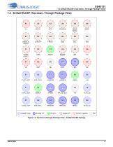
1.2 42-Ball WLCSP (Top-down, Through-Package View) 1.2 42-Ball WLCSP (Top-down, Through-Package View) Charge Pump Power Supplies Figure 1-2. Top-Down (Through-Package) View—42-Ball WLCSP Package

 Open the catalog to page 5
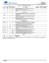
CS43131-7

I.The power supply is determined by ADPT_PWR setting (see Section 4.3.1). VP is used if ADPT_PWR = 001 (VP_LDO Mode) or when necessary for ADPTPWR = 111 (Adapt-to-Signal Mode).

 Open the catalog to page 7
CS43131-8

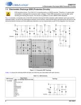
1.4 Electrostatic Discharge (ESD) Protection Circuitry 1.4 Electrostatic Discharge (ESD) Protection Circuitry ESD-sensitive device. The CS43131 is manufactured on a CMOS process. Therefore, it is generically susceptible to damage from excessive static voltages. Proper ESD precautions must be taken while handling and storing this device. This device is qualified to current JEDEC ESD standards. Fig. 1-3 provides a composite view of the ESD domains showing the ESD protection paths between each pad and the substrate (GND), as well as the interrelations between some domains. Note that this figure...

 Open the catalog to page 8
CS43131-9

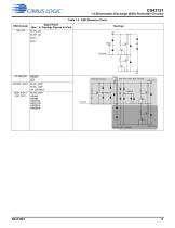
CIRRUS LOGIC CS431311.4 Electrostatic Discharge (ESD) Protection Circuitry Table 1-2. ESD Domains (Cont.) ESD Domain

 Open the catalog to page 9
CS43131-10

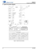
2 Typical Connection Diagram 2 Typical Connection Diagram VL Audio Codec Headphone Output Applications Processor/ MicroController HPOUTB Headphone Connector HP_DETECT RESET PCM/DoP Digital Audio Source DoP/DSD Digital Audio Source Audio Devices Note 1 All external passive component values shown are nominal . Clocking Configuration XTAL External MCLK System Clock Key for Capacitor Types Required : * Use low ESR, X7R/X5R capacitors If no type symbol is shown next to a capacitor, any type may be used. ** Use C0G capacitors. VCP_FILT Configuration EXT_VCPFILT = 0 VCP_FILT+ VCP_FILT– GNDCP VCP_FILT+...

 Open the catalog to page 10
*Prices are pre-tax. They exclude delivery charges and customs duties and do not include additional charges for installation or activation options. Prices are indicative only and may vary by country, with changes to the cost of raw materials and exchange rates.