- Catalogs
- Cirrus Logic
- CS35L00/01/03
CS35L00/01/03
1 /34Pages

CS35L00/01/03
1 /34Pages
Catalog excerpts

CS35L00 2.8 W Mono Class-D Audio Amplifier with Low Idle Current CS35L00 Features General Description Hybrid Class-D Architecture The CS35L00 is a 2.8 W high efficiency Hybrid Class-D audio amplifier with low idle current consumption and a selectable gain. – <1 mA Quiescent Current – 1 x 2.8 W into 4 Ω (10% THD+N) – 1 x 2.3 W into 4 Ω (1% THD+N) – 1 x 1.7 W into 8 Ω (10% THD+N) – 1 x 1.4 W into 8 Ω (1% THD+N) Advanced ΔΣ Closed-loop Modulation – 98 dB Signal-to-Noise Ratio (A-Weighted) – 0.02% THD+N @ 1 W (SD & HD Mode) Integrated Protection and Automatic Recovery for Output Short-circuit and Thermal Overload Thermally Enhanced 10-pin DFN Package with Pin-selectable Gain of +6 dB or +12 dB Pop and Click Suppression The CS35L00 features an advanced closed-loop architecture to provide 0.02% THD+N at 1 W and -88 dB PSRR at 217 Hz. A flexible Hybrid Class-D output stage offers four modes of operation: Standard Class-D (SD) mode offers full audio bandwidth and high audio performance; Hybrid Class-D (HD) mode offers a substantial reduction in idle power consumption with an integrated ClassH controller; Reduced Frequency Class-D (FSD) mode reduces the output switching frequency, producing lower electromagnetic interference (EMI); and Reduced Frequency Hybrid Class-D (FHD) mode produces both the lower idle power consumption of HD mode and the reduced EMI benefits of FSD mode. Common Applications Requiring minimal external components and PCB space, the CS35L00 is available in a 3.0 mm x 3.0 mm, 10-pin DFN package in Commercial grade (-10°C to +70°C). Please see “Ordering Information” on page 33 for package options and gain configurations. Laptops Netbooks Portable Navigation Devices Active Speakers Portable Gaming Class-H Controller Low Drop-Out Voltage Regulator Shutdown Gate Drivers Audio In + Gain Advanced ΔΣ Modulator Gain Select Speaker Out + Speaker Out Gate Drivers Internal Oscillator Short Circuit/Thermal Protection Preliminary Product Information http://www.cirrus.com This document contains information for a new product. Cirrus Logic reserves the right to modify this product without notice. Copyright Cirrus Logic, In
Open the catalog to page 1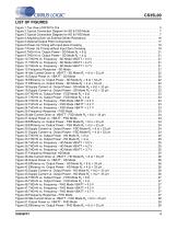
CS35L00 LIST OF FIGURES Figure 1.Top View of DFN Pin Out . . . . . . . . . . . . . . . . . . . . . . . . . . . . . . . . . . . . . . . . . . . . . . . . . . . . . . . . . . . . . 5 Figure 2.Typical Connection Diagram for SD & FSD Mode . . . . . . . . . . . . . . . . . . . . . . . . . . . . . . . . . . . . . . . . . . 7 Figure 3.Typical Connection Diagram for HD & FHD Mode . . . . . . . . . . . . . . . . . . . . . . . . . . . . . . . . . . . . . . . . . . 7 Figure 4.Adjusting Gain via External Series Resistance . . . . . . . . . . . . . . . . . . . . . . . . . . . . . . . . . . . . . . . . . ....
Open the catalog to page 3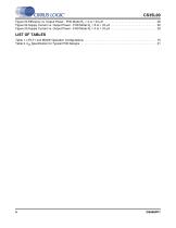
CS35L00 Figure 53.Efficiency vs. Output Power - FHD Mode RL = 4 Ω + 33 μH . . . . . . . . . . . . . . . . . . . . . . . . . . . . . . . . . 28 Figure 54.Supply Current vs. Output Power - FHD Mode RL = 8 Ω + 33 μH . . . . . . . . . . . . . . . . . . . . . . . . . . . . 28 Figure 55.Supply Current vs. Output Power - FHD Mode RL = 4 Ω + 33 μH . . . . . . . . . . . . . . . . . . . . . . . . . . . . 28 LIST OF TABLES Table 1. LFILT+ and MODE Operation Configurations . . . . . . . . . . . . . . . . . . . . . . . . . . . . . . . . . . . . . . . . . . . . . 15 Table 2. θJA Specification for Typical PCB...
Open the catalog to page 4
Figure 1. Top View of DFN Pin Out (Looking down through package) Shutdown (Input) - Pulling this pin low places the CS35L00 in shutdown. Negative Analog Input (Input) - Differential negative audio signal input Low Drop Out Regulator Filter (Output) - Bypass capacitor connection point for internal LDO. Connecting this net to VBATT places the device into SD mode. Positive Analog Input (Input) - Differential positive audio signal input. Switching Mode (Input) - Controls the output switching modes of the CS35L00. Negative PWM Output (Output) - Differential negative PWM output. Gain Select (Input)...
Open the catalog to page 5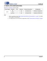
CS35L00 2. DIGITAL PIN CONFIGURATIONS See (Note 1) and (Note 2) below the table. Power Supply Internal Connections Hysteresis on CMOS Input Hysteresis on CMOS Input Hysteresis on CMOS Input Note: 1. Refer to specification table “Digital Interface Specifications & Characteristics” on page 14 for details on the digital I/O characteristics. 2. I/O voltage levels must not exceed the voltage listed in table “Absolute Maximum Ratings” on page 8.
Open the catalog to page 6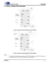
System Controller GAIN_SEL Connect to VBATT for +6dB Gain or GND for +12dB Gain Figure 2. Typical Connection Diagram for SD & FSD Mode 2.5V - 5V System Controller Connect to VBATT for +6dB Gain or GND for +12dB Gain Figure 3. Typical Connection Diagram for HD & FHD Mode Note: 3. The value of the capacitance connected to the LFILT+ net should not exceed 4.7 μF. Presence of a capacitance above 4.7 μF will prevent proper HD and FHD operation.
Open the catalog to page 7
CS35L00 4. CHARACTERISTICS & SPECIFICATIONS Test Conditions (unless otherwise specified): GND = 0 V; All voltages with respect to ground; Input signal = 997 Hz differential sine wave; TA = 25°C; VBATT = 5.0 V; RL = 8 Ω; 22 Hz to 20 kHz measurement bandwidth; Measurements taken with AES17 measurement filter and Audio Precision AUX-0025 passive filter. RECOMMENDED OPERATING CONDITIONS GND = 0 V; All voltages with respect to ground. Please see (Note 4). Ambient Temperature Junction Temperature DC Power Supply Supply Voltage ABSOLUTE MAXIMUM RATINGS GND = 0 V; All voltages with respect to ground....
Open the catalog to page 8
CS35L00 ELECTRICAL CHARACTERISTICS - ALL OPERATIONAL MODES Parameters GAIN_SEL = Low (12 dB) GAIN_SEL = High (6 dB) Vrms Vrms Input Level for Entering VBATT Operation in GAIN_SEL = Low (12 dB) V HD/FHD Modes (Note 9) IN-VBATT GAIN_SEL = High (6 dB) Vrms Vrms GAIN_SEL = Low GAIN_SEL = High Max. Current from LFILT+ LFILT+ Output Impedance VBATT Limit for HD/FHD Mode Input Level for Entering LDO Operation in HD/FHD Modes (Note 8) LDO Entry Time Delay LDO Level for HD/FHD Modes Test Conditions VOFFSET Inputs AC coupled to GND Output Offset Voltage Amplifier Gain Shutdown Supply Current Thermal Error...
Open the catalog to page 9All Cirrus Logic catalogs and technical brochures


Archived catalogs
 CS48DV2/6
2 Pages
 Mixed-Signal Audio Brochure
64 Pages


- Signal amplifying integrated circuit
- Power amplifying integrated circuit
- Compact converter
- Serial converter
- Industrial converter
- Measuring amplifier
- Voltage amplifier
- Serial receiver
- Digital amplifier
- Power converter
- Microcontroller
- Current amplifier
- Digital converter
- Isolated converter
- Digital receiver
- Analog converter
- Fast converter
- Programmable converter
- Analog receiver